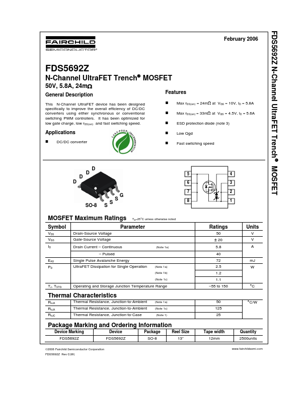
GENERAL DESCRIPTION
FEATURES
Max rDS(on) = 24mΩ at VGS = 10V, ID = 5.8A Max rDS(on) = 33mΩ at VGS = 4.5V, ID = 5.6A ESD protection diode (note 3) APPLICATIONS
Low Qgd DC/DC converter Fast switching speed D D D D SO-8 G SS S 5 6 7 8 MOSFET MAXIMUM RATINGS
TA=25oC unless otherwise noted Symbol VDS VGS ID Drain-Source Voltage Parameter Gate-Source Voltage Drain Current – Continuous (Note 1a) – Pulsed EAS Single Pulse Avalanche Energy PD UltraFET Dissipation for Single Operation (Note 1a) (Note 1b) (Note 1c) TJ, TSTG Operating and Storage Junction Temperature Range Thermal Characteristics RθJA Thermal Resistance, Junction-to-Ambient RθJA Thermal Resistance, Junction-to-Ambient RθJC Thermal Resistance, Junction-to-Case (Note 1a) (Note 1c) (Note 1) Package Marking and Ordering Information Device Marking Device Package Reel Size FDS5692Z FDS5692Z SO-8 13” ©2006 Fairchild Semiconductor Corporation FDS5692Z Rev C(W) 4 3 2 1 Ratings 50 ± 20 5.8 40 72 2.5 1.2 1.1 –55 to 150 50 125 25... Fairchild Semiconductor