FDS6912
Overview
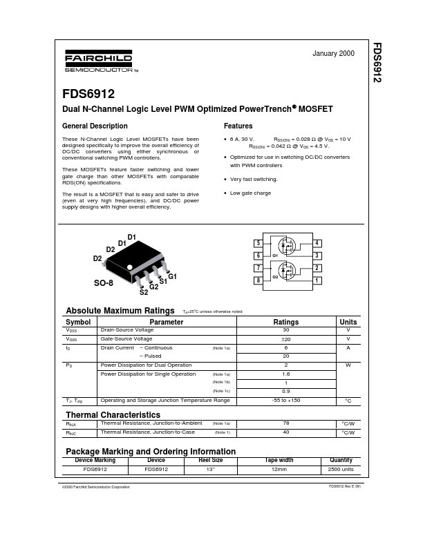
These N-Channel Logic Level MOSFETs have been designed specifically to improve the overall efficiency of DC/DC converters using either synchronous or conventional switching PWM controllers. These MOSFETs feature faster switching and lower gate charge than other MOSFETs with comparable RDS(ON) specifications.
- 6 A, 30 V. RDS(ON) = 0.042 Ω @ VGS = 4.5 V.
- Optimized for use in switching DC/DC converters with PWM controllers
- Very fast switching.
- Low gate charge