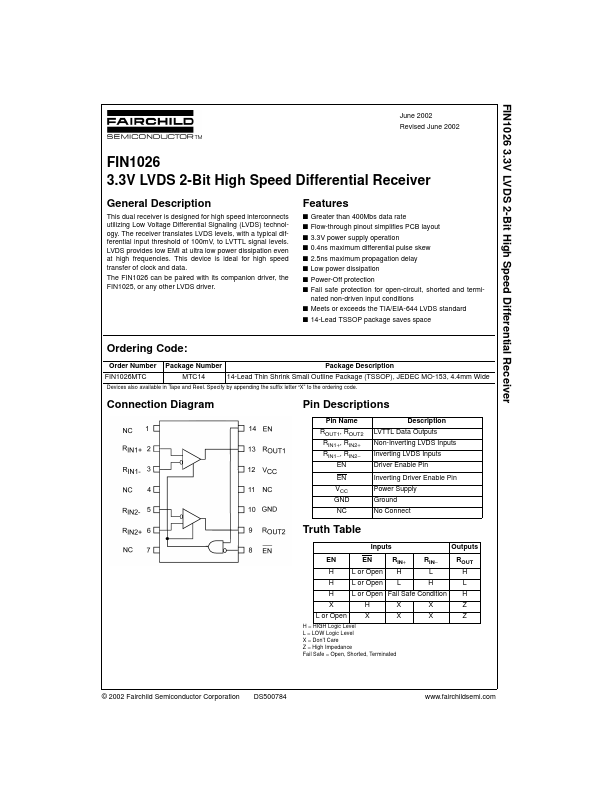
FIN1026
FIN1026 is 3.3V LVDS 2-Bit High Speed Differential Receiver manufactured by Fairchild Semiconductor.
FIN1026 3.3V LVDS 2-Bit High Speed Differential Receiver
June 2002 Revised June 2002
FIN1026 3.3V LVDS 2-Bit High Speed Differential Receiver
General Description
This dual receiver is designed for high speed interconnects utilizing Low Voltage Differential Signaling (LVDS) technology. The receiver translates LVDS levels, with a typical differential input threshold of 100m V, to LVTTL signal levels. LVDS provides low EMI at ultra low power dissipation even at high frequencies. This device is ideal for high speed transfer of clock and data. The FIN1026 can be paired with its panion driver, the FIN1025, or any other LVDS driver.
Features s Greater than 400Mbs data rate s Flow-through pinout simplifies PCB layout s 3.3V power supply operation s 0.4ns maximum differential pulse skew s 2.5ns maximum propagation delay s Low power dissipation s Power-Off protection s Fail safe protection for open-circuit, shorted and terminated non-driven input conditions s Meets or exceeds the TIA/EIA-644 LVDS standard s 14-Lead TSSOP package saves space
Ordering Code:
Order Number FIN1026MTC Package Number MTC14 Package Description 14-Lead Thin Shrink Small Outline Package (TSSOP), JEDEC MO-153, 4.4mm Wide
Devices also available in Tape and Reel. Specify by appending the suffix letter “X” to the ordering code.
Connection Diagram
Pin Descriptions
Pin Name ROUT1, ROUT2 RIN1+, RIN2+ RIN1- , RIN2- EN EN VCC GND NC Description LVTTL Data Outputs Non-Inverting LVDS Inputs Inverting LVDS Inputs Driver Enable Pin Inverting Driver Enable Pin Power Supply Ground No Connect
Truth Table
Inputs EN H H H X L or Open EN L or Open L or Open H X RIN+ H L X X RIN- L H X X Outputs ROUT H L H Z Z
L or Open Fail Safe Condition
H = HIGH Logic Level L = LOW Logic Level X = Don’t Care Z = High Impedance Fail Safe = Open, Shorted, Terminated
© 2002 Fairchild Semiconductor Corporation
DS500784
.fairchildsemi....