Datasheet4U.com
🌙
FJD5555 Datasheet | Fairchild Semiconductor
Part:
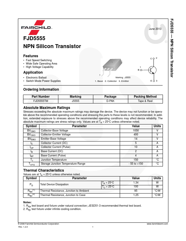
FJD5555
Description:
NPN Silicon Transistor
Category:
Transistor
Manufacturer:
Fairchild Semiconductor
Size:
294.60 KB
FJD5555 Datasheet (PDF) Download
Fairchild Semiconductor
FJD5555
Key Features
Fast Speed Switching
Wide Safe Operating Area
High Voltage Capability
Datasheets by Manufacturer
Part Number
Manufacturer
Description
FJD5555
Inchange Semiconductor
NPN Transistor
×
Close