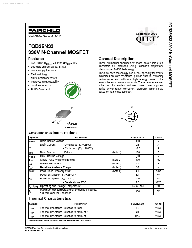
FQB25N33
FQB25N33 is N-Channel MOSFET manufactured by Fairchild Semiconductor.
Features
- 25A, 330V, RDS(on) = 0.23Ω @VGS = 10V
- Low gate charge (typical 58n C)
- Low Crss (typical 40p F)
- Fast switching
- 100% avalanche tested
- Improved dv/dt capability
- Ro HS pliant
REE I DF
September 2006 ®
General Description
These N-Channel enhancement mode power field effect transistors are produced using Farichild’s proprietary, planar stripe, DMOS technology. This advanced technology has been especially tailored to minimized on-state resistance, provide superior switching performance, and withstand high energy pulse in the avalanche and mutation mode. These devices are well suited for high efficient switched mode power supplies, active power factor correction, electronic lamp ballast based on half bridge topology.
- Qualified to AEC Q101
Absolute Maximum Ratings
Symbol VDSS Drain-Source Voltage ID IDM VGSS EAS IAR EAR dv/dt PD Drain Current Drain Current Parameter FQB25N33 330 25 16.0 (Note 1) (Note 2) (Note 1) (Note 1) (Note 3) 100 ±30 370 25 37 4.5 3.1 250 2.0 -55 to +150 300 Units V A A A V m J A m J V/ns W W W/o C o o
- Continuous (TC = 25o C)
- Continuous (TC = 100o C)
M ENTATIO LE N MP
- Pulsed
Gate -Source Voltage Single Pulse Avalanche Energy Avalanche Current Repetitive Avalance Energy Peak Diode Recovery dv/dt Power Dissipation (TA = 25o C)
- Power Dissipation (TC = 25o C)
- Derate above 25o C
TJ, TSTG Operating and Storage Temperature TL Maximum lead temperature for soldering purposes, 1/8 from case for 5 seconds
Thermal Characteristics
Symbol RθJC RθJA RθJA Parameter Thermal Resistance, Junction to Case Thermal Resistance, Junction to Ambient
- Thermal Resistance, Junction to Ambient FQB25N33 0.5 40 62.5 Units o o o
C/W C/W C/W
- When mounted on the minimum pad size remended (PCB Mount)
©2006 Fairchild Semiconductor Corporation FQB25N33 Rev. A
.fairchildsemi.
FQB25N33 330V N-Channel MOSFET
Package Marking and Ordering Information
Device Marking
Device
Package
D2-PAK...