P4N60 Overview
Key Specifications
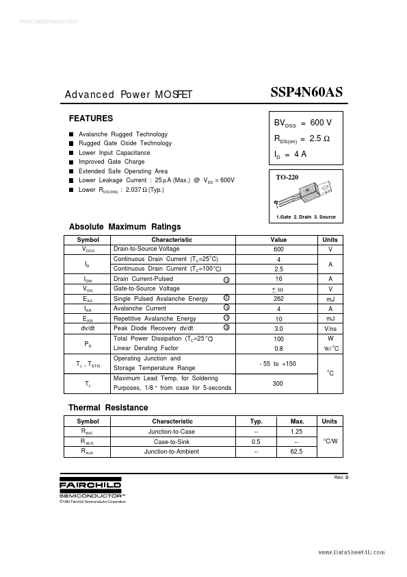
Package: TO-220
Mount Type: Through Hole
Pins: 3
Height: 16.51 mm
| Part | P4N60 |
|---|---|
| Description | SSP4N60 |
| Manufacturer | Fairchild Semiconductor |
| Size | 290.43 KB |
Package: TO-220
Mount Type: Through Hole
Pins: 3
Height: 16.51 mm
| Seller | Inventory | Price Breaks | Buy |
|---|---|---|---|
| Rochester Electronics | 6909 | 100+ : 1.32 USD 500+ : 1.19 USD 1000+ : 1.1 USD 10000+ : 0.9768 USD |
View Offer |
| Rochester Electronics | 1260 | 100+ : 1.32 USD 500+ : 1.19 USD 1000+ : 1.1 USD 10000+ : 0.9768 USD |
View Offer |
| Part Number | Manufacturer | Description |
|---|---|---|
| HFDOM44P-xxxSx | Hanbit Electronics | 44Pin Flash Disk Module |
| HFDOM40B-xxxSx | Hanbit Electronics | 40Pin Flash Disk Module |
| CP2105 | Silicon Labs | SINGLE-CHIP USB TO DUAL UART BRIDGE |