SFU9230B
SFU9230B is 200V P-Channel MOSFET manufactured by Fairchild Semiconductor.
Description
These P-Channel enhancement mode power field effect transistors are produced using Fairchild’s proprietary, planar, DMOS technology. This advanced technology has been especially tailored to minimize on-state resistance, provide superior switching performance, and withstand high energy pulse in the avalanche and mutation mode. These devices are well suited for high efficiency switching DC/DC converters.
Features
- -
- -
- - -5.4A, -200V, RDS(on) = 0.8Ω @VGS = -10 V Low gate charge ( typical 33 n C) Low Crss ( typical 45 p F) Fast switching 100% avalanche tested Improved dv/dt capability
S D G!
!
- -
▶ ▲
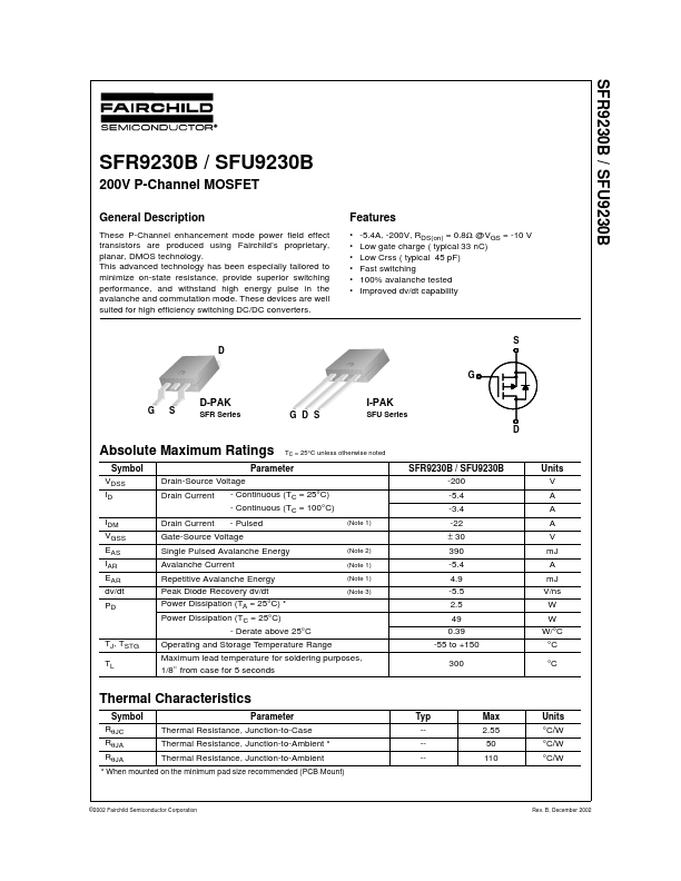
D-PAK
SFR Series
I-PAK
SFU Series
- !
Absolute Maximum Ratings
Symbol VDSS ID IDM VGSS EAS IAR EAR dv/dt PD
TC = 25°C unless otherwise noted
Parameter Drain-Source Voltage
- Continuous (TC = 25°C) Drain Current
- Continuous (TC = 100°C) Drain Current
- Pulsed
(Note 1)
SFR9230B / SFU9230B -200 -5.4 -3.4 -22 ± 30
(Note 2) (Note 1) (Note 1) (Note 3)
Units V A A A V m J A m J V/ns W W W/°C °C °C
Gate-Source Voltage Single Pulsed Avalanche Energy Avalanche Current Repetitive Avalanche Energy Peak Diode Recovery dv/dt Power Dissipation (TA = 25°C)
- Power Dissipation (TC = 25°C)
390 -5.4 4.9 -5.5 2.5 49 0.39 -55 to +150 300
TJ, TSTG TL
- Derate above 25°C Operating and Storage Temperature Range Maximum lead temperature for soldering purposes, 1/8" from case for 5 seconds
Thermal Characteristics
Symbol RθJC RθJA RθJA Parameter Thermal Resistance, Junction-to-Case Thermal Resistance, Junction-to-Ambient
- Thermal Resistance, Junction-to-Ambient Typ ---Max 2.55 50 110 Units °C/W °C/W °C/W
- When mounted on the minimum pad size remended (PCB Mount)
©2002 Fairchild Semiconductor...