SSD2025 Overview
Key Specifications
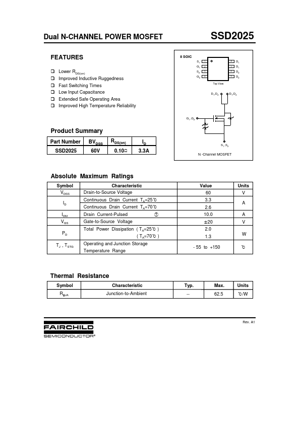
Package: SOIC
Mount Type: Surface Mount
Pins: 8
Max Operating Temp: 150 °C
Key Features
- Improved Inductive Ruggedness !
- Fast Switching Times !
- Low Input Capacitance !
- Extended Safe Operating Area !
| Part | SSD2025 |
|---|---|
| Description | Dual N-CHANNEL POWER MOSFET |
| Category | MOSFET |
| Manufacturer | Fairchild Semiconductor |
| Size | 183.66 KB |
Package: SOIC
Mount Type: Surface Mount
Pins: 8
Max Operating Temp: 150 °C
| Seller | Inventory | Price Breaks | Buy |
|---|---|---|---|
| Verical | 3000 | 765+ : 0.4905 USD 1000+ : 0.4524 USD 10000+ : 0.4033 USD 100000+ : 0.3379 USD |
View Offer |
| Rochester Electronics | 3002 | 100+ : 0.436 USD 500+ : 0.3924 USD 1000+ : 0.3619 USD 10000+ : 0.3226 USD |
View Offer |
| Part Number | Manufacturer | Description |
|---|---|---|
| A2SHB | HAOHAI | N-Channel MOSFET |
| AP9563GH | Advanced Power Electronics Corp | P-CHANNEL ENHANCEMENT MODE POWER MOSFET |
| FCPF360N65S3R0L | onsemi | N-Channel MOSFET |