74F651
74F651 is Transceivers/Registers manufactured by Fairchild Semiconductor.
Description
These devices consist of bus transceiver circuits with Dtype flip-flops, and control circuitry arranged for multiplexed transmission of data directly from the input bus or from internal registers. Data on the A or B bus will be clocked into the registers as the appropriate clock pin goes to HIGH logic level. Output Enable pins (OEAB, OEBA) are provided to control the transceiver function.
Features s Independent registers for A and B buses s Multiplexed real-time and stored data s Choice of non-inverting and inverting data paths 74F651 inverting 74F652 non-inverting
Ordering Code:
Order Number 74F651SC 74F651SPC 74F652SC 74F652SPC Package Number M24B N24C M24B N24C Package Description
24-Lead Small Outline Integrated Circuit (SOIC), JEDEC MS-013, 0.300 Wide 24-Lead Plastic Dual-In-Line Package (PDIP), JEDEC MS-100, 0.300 Wide 24-Lead Small Outline Integrated Circuit (SOIC), JEDEC MS-013, 0.300 Wide 24-Lead Plastic Dual-In-Line Package (PDIP), JEDEC MS-100, 0.300 Wide
Devices also available in Tape and Reel. Specify by appending the suffix letter “X” to the ordering code.
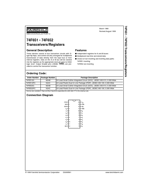
Connection Diagram
© 1999 Fairchild Semiconductor Corporation
DS009581
.fairchildsemi.
- 74F652
Logic Symbols
74F651 74F652
IEEE/IEC 74F651
IEEE/IEC 74F652
Unit Loading/Fan Out
Pin Names A0- A7, B0- B7 CPAB, CPBA SAB, SBA OEAB, OEBA Description
A and B Inputs/ 3-STATE Outputs Clock Inputs Select Inputs Output Enable Inputs U.L. HIGH/LOW 1.0/1.0 600/106.6 (80) 1.0/1.0 1.0/1.0 1.0/1.0 Input IIH/IIL Output IOH/IOL 20 µA/- 0.6 m A
- 12 m A/64 m A (48 m A) 20 µA/- 0.6 m A 20 µA/- 0.6 m A 20 µA/- 0.6 m A
Function Table
Inputs OEAB OEBA CPAB CPBA SAB SBA L L X H L L L L H H H H H H H X L L L H H L H or L H or L H or L Inputs/Outputs (Note 1) A0 thru A7 Input Input Input Output Output Input Output B0 thru B7 Input Operating Mode Isolation Store A and B Data Not Specified Store A, Hold B Output Input Input Output Output Store A in Both Registers Hold A, Store B Store B in Both Registers...