74F651
74F651 is Transceivers/Registers manufactured by National Semiconductor.
Description
These devices consist of bus transceiver circuits with D-type flip-flops and control circuitry arranged for multiplexed transmission of data directly from the input bus or from internal registers Data on the A or B bus will be clocked into the registers as the appropriate clock pin goes to HIGH logic level Output Enable pins (OEAB OEBA) are provided to control the transceiver function
Features
Independent registers for A and B buses Multiplexed real-time and stored data Choice of non-inverting and inverting data paths ’F651 inverting ’F652 non-inverting Guaranteed 4000V minimum ESD protection mercial 74F651SPC
Military
Package Number N24C
Package Description
24-Lead (0 300 Wide) Molded Dual-In-Line 24-Lead (0 300 Wide) Ceramic Dual-In-Line 24-Lead (0 300 Wide) Molded Small Outline JEDEC 24-Lead Cerpack 24-Lead Ceramic Leadless Chip Carrier Type C 24-Lead (0 300 Wide) Molded Dual-In-Line 24-Lead (0 300 Wide) Ceramic Dual-In-Line 24-Lead (0 300 Wide) Molded Small Outline JEDEC 24-Lead Cerpack 24-Lead Ceramic Leadless Chip Carrier Type C
54F651SDM (Note 2) 74F651SC (Note 1) 54F651FM (Note 2) 54F651LM (Note 2) 74F652SPC 54F652SDM (Note 2) 74F652SC (Note 1) 54F652FM (Note 2) 54F652LM (Note 2)
Note 1 Devices also available in 13 reel Use suffix e SCX
J24F M24B W24C E28A N24C J24F M24B W24C E28A
Note 2 Military grade device with environmental and burn-in processing Use suffix e DMQB FMQB and LMQB
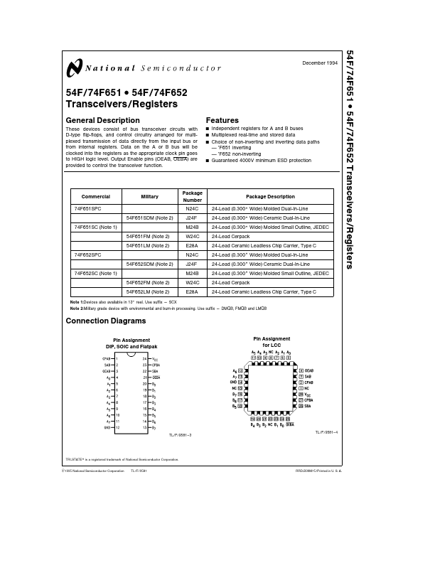
Connection Diagrams
Pin Assignment DIP SOIC and Flatpak Pin Assignment for LCC
TL F 9581
- 3
TL F 9581
- 4
TRI-STATE is a registered trademark of National Semiconductor Corporation C1995 National Semiconductor Corporation
TL F 9581
RRD-B30M75 Printed in U S A
Logic Symbols
IEEE IEC ’F651 IEEE IEC ’F652
TL F 9581- 1
TL F 9581
- 10
’F651
’F652
TL F 9581
- 11 TL F 9581- 2
Unit Loading Fan Out
54F 74F Pin Names Description
UL HIGH LOW Input IIH IIL Output IOH IOL
A0
- A7 B0
- B7 A and B Inputs 10 10 20 m A b0 6 m A TRI-STATE Outputs 600 106 6...