NDS9933A
Description
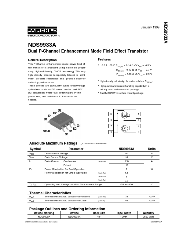
This P-Channel enhancement mode power field effect transistor is produced using Fairchild’s proprietary, high cell density, DMOS technology.
Key Features
- 2.8 A, -20 V. RDS(on) = 0.14 Ω @ VGS = -4.5 V RDS(on) = 0.19 Ω @ VGS = -2.7 V RDS(on) = 0.20 Ω @ VGS = -2.5 V
- High density cell design for extremely low RDS(on)
- High power and current handling capability in a
- Dual MOSFET in surface mount package