SSP6N70A
SSP6N70A is Advanced Power MOSFET manufactured by Fairchild Semiconductor.
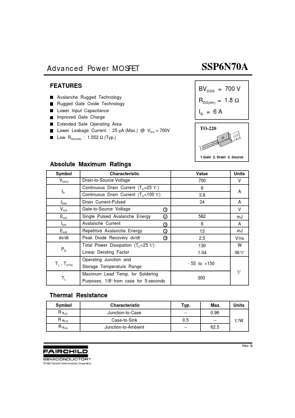
FEATURES
Avalanche Rugged Technology Rugged Gate Oxide Technology Lower Input Capacitance Improved Gate Charge Extended Safe Operating Area Lower Leakage Current : 25 µA (Max.) @ VDS = 700V Low RDS(ON) : 1.552 Ω (Typ.)
1 2 3
BVDSS = 700 V RDS(on) = 1.8 Ω ID = 6 A
TO-220
1.Gate 2. Drain 3. Source
Absolute Maximum Ratings
Symbol VDSS ID IDM VGS EAS IAR EAR dv/dt PD TJ , TSTG TL Characteristic Drain-to-Source Voltage Continuous Drain Current (TC=25 C ) Continuous Drain Current (TC=100 C) Drain Current-Pulsed Gate-to-Source Voltage Single Pulsed Avalanche Energy Avalanche Current Repetitive Avalanche Energy Peak Diode Recovery dv/dt Total Power Dissipation (TC=25 C) Linear Derating Factor Operating Junction and Storage Temperature Range Maximum Lead Temp. for Soldering Purposes, 1/8“ from case for 5-seconds
Ο Ο Ο
Value 700 6 3.8 24
1 O 2 O 1 O 1 O 3 O
Units V A A V m J A m J V/ns W W/ C
Ο
582 6 13 2.5 130 1.04
- 55 to +150
Ο
Thermal Resistance
Symbol R θJC R θCS R θJA Characteristic Junction-to-Case Case-to-Sink Junction-to-Ambient Typ. -0.5 -Max. 0.96 -62.5
Ο
Units
C/W
Rev. B
©1999 Fairchild Semiconductor Corporation
Electrical Characteristics (TC=25 C unless otherwise specified)
Ο
N-CHANNEL POWER MOSFET
Symbol BVDSS ∆BV/∆TJ VGS(th) IGSS IDSS RDS(on) gfs Ciss Coss Crss td(on) tr td(off) tf Qg Qgs Qgd
Characteristic Drain-Source Breakdown Voltage Breakdown Voltage Temp. Coeff. Gate Threshold Voltage Gate-Source Leakage , Forward Gate-Source Leakage , Reverse Drain-to-Source Leakage Current Static Drain-Source On-State Resistance Forward Transconductance Input Capacitance Output Capacitance Reverse Transfer Capacitance Turn-On Delay Time Rise Time Turn-Off Delay Time Fall Time Total Gate Charge Gate-Source Charge Gate-Drain(“ Miller” ) Charge
Min. Typ. Max. Units 700 -2.0 -----------------0.79 ------4.12 100 45 18 23 76 26 51 8.3 23.1 --4.0 100 -100 25 250 1.8 -115 55 45 55 160 60 67 --n C ns
µA
Test Condition VGS=0V,ID=250 µA...