FMS2022
FMS2022 is MMIC SP4T Absorptive Switch manufactured by Filtronic.
Features
:
- -
- -
- Available in die form Suitable for WLAN Applications Low Insertion loss <1.3 d B at 4 GHz typical High isolation >30 d B at 4 GHz typical Absorptive
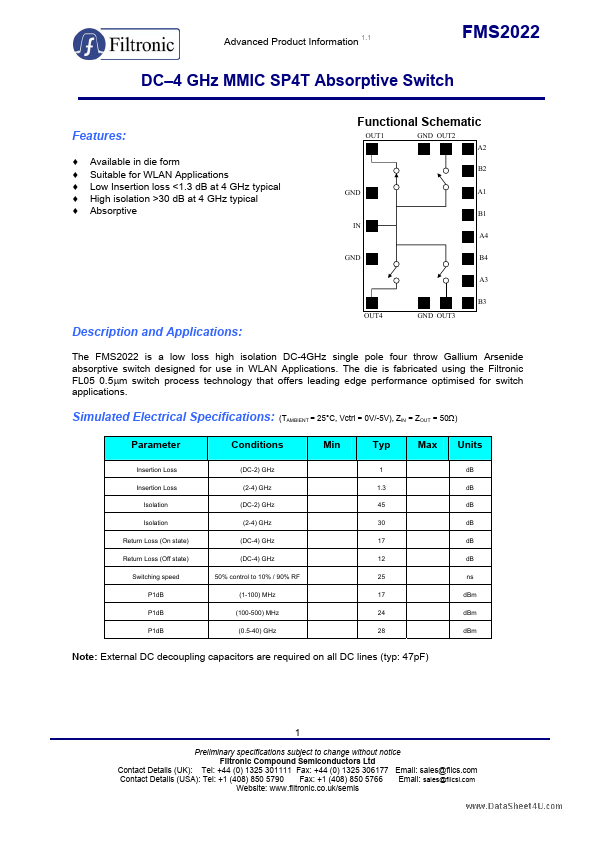
OUT1 GND OUT2 A2 B2 GND A1 B1 IN A4 GND B4 A3 B3 OUT4 GND OUT3
Description and Applications:
The FMS2022 is a low loss high isolation DC-4GHz single pole four throw Gallium Arsenide absorptive switch designed for use in WLAN Applications. The die is fabricated using the Filtronic FL05 0.5µm switch process technology that offers leading edge performance optimised for switch applications.
Simulated Electrical Specifications:
Parameter
Insertion Loss Insertion Loss Isolation Isolation Return Loss (On state) Return Loss (Off state) Switching speed P1d B P1d B P1d B
(TAMBIENT = 25°C, Vctrl = 0V/-5V), ZIN = ZOUT = 50Ω)
Conditions
(DC-2) GHz (2-4) GHz (DC-2) GHz (2-4) GHz (DC-4) GHz (DC-4) GHz 50% control to 10% / 90% RF (1-100) MHz (100-500) MHz (0.5-40) GHz
Min
Typ
1 1.3 45 30 17 12 25 17 24 28
Max
Units d B d B d B d B d B d B ns d Bm d Bm d Bm
Note: External DC decoupling capacitors are required on all DC lines (typ: 47p F)
Preliminary specifications subject to change without notice Filtronic pound Semiconductors Ltd Contact Details (UK): Tel: +44 (0) 1325 301111 Fax: +44 (0) 1325 306177 Email: sales@filcs. Contact Details (USA): Tel: +1 (408) 850 5790 Fax: +1 (408) 850 5766 Email: sales@filcsi. Website: .filtronic.co.uk/semis
Advanced Product Information 1.1
Truth Table:
Control Lines RF Path
A1 B1 A2 B2 A3 B3 A4 B4 IN-OUT1 IN-OUT2 IN-OUT3 IN-OUT4
-5V 0V 0V 0V 0V -5V -5V -5V 0V -5V 0V 0V -5V 0V -5V -5V 0V 0V -5V 0V -5V -5V 0V -5V 0V 0V 0V -5V -5V -5V -5V 0V ON OFF OFF OFF OFF ON OFF OFF OFF OFF ON OFF OFF OFF OFF ON
Note: -5V ± 0.5V, 0V+0.5V
Pad Layout:
OUT1 GND1 OUT2 A2 B2 GND3 A1 B1 IN GND4 A4 B4 A3 B3 OUT4 GND2 OUT3
Pad Reference
IN OUT1 OUT2 OUT3 OUT4 A1 B1 A2 B2 A3 B3 A4 B4 GND1 GND2 GND3 GND4
Description
RFIN RFOUT1 RFOUT2 RFOUT3 RFOUT4 A1 B1 A2 B2 A3 B3 A4 B4 GND GND GND GND
Pin...