FP6601
FP6601 is USB Dedicated Charging Port Controller manufactured by Fitipower.
Description
The FP6601 is a fast charge protocol controller and follows Quick Charge 2.0 specification for smart power bank application. The protocol feature monitors USB D+/D- data line voltage, and automatically adjusts output voltage of power bank and wall adaptor to optimize charge time.
FP6601 is a high performance solution for fast-charging mechanism and it saves charging time. It supports the full output voltage range of either Class A.
FP6601 can support not only USB BC pliant devices, but also Apple / Samsung devices and automatically detects whether a connected powered device (PD) is Quick Charge 2.0 capable before enabling output voltage adjustment. If a PD not pliant to Quick Charge 2.0 is detected the FP6601 disables output voltage adjustment to ensure safe operation with legacy 5 V only USB PDs.
The FP6601 is available in a space-saving SOT-23-6 package.
Features
- Input Voltage Range from 4V to 6V.
- Fully Supports Quick Charge 2.0 specification:
Class A: 5V/9V/12V Output Voltage.
- Supports USB DCP Shorting D+ Line to D- Line per USB Battery Charging Specification, Revision 1.2.
- Meets Chinese Telemunication Industrial Standard YD/T 1591-2009
- Supports USB DCP applying 2.7V on D+ line and 2.7V on D- line.
- Supports USB DCP applying 1.2V on D+ and Dlines
- Automatic selection of D+/D- mode for an attached device
- plaint with Apple® and Samsung devices
- SOT-23-6 package.
Applications
- Wall-Adapter / Power Plugs, Outlets
- Mobile / Tablet Power Bank
- Car Charger
- USB Power Output Ports
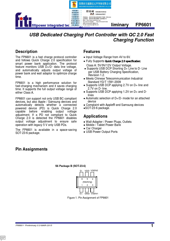
Pin Assignments
S6 Package B (SOT-23-6)
D- VDD VSEN2
(Marking)
D+ GND VSEN1
Figure 1. Pin Assignment of FP6601
FR6601- Preliminary 0.3-MAR-2015
1 fitipower integrated technology lnc.
S6 Package B (SOT-23-6)
Typical Application Circuit
Preliminary FP6601
Feedback Node
VOUT
RVDD
R1 RSEN2 4 VSEN2
VDD...