AO8806
AO8806 is Dual N-Channel FET manufactured by Freescale Semiconductor.
General Description mon-Drain Dual N-Channel Enhancement Mode Field Effect Transistor
The AO8806 uses advanced trench technology to provide excellent RDS(ON) , low gate charge and operation with gate voltages as low as 1.8V. This device is suitable for use as a uni-directional or bidirectional load switch, facilitated by its mon- drain configuration.
Features
VDS (V) = 20V ID = 6 A RDS(ON) < 25mΩ (VGS = 4.5V) RDS(ON) < 30mΩ (VGS = 2.5V) RDS(ON) < 40mΩ (VGS = 1.8V)
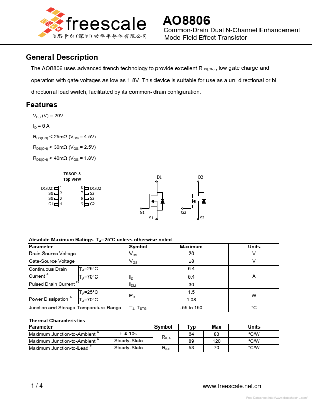
TSSOP-8 Top View D1/D2 S1 S1 G1 1 2 3 4 8 7 6 5 D1/D2 S2 S2 G2 G1 S1 G2...