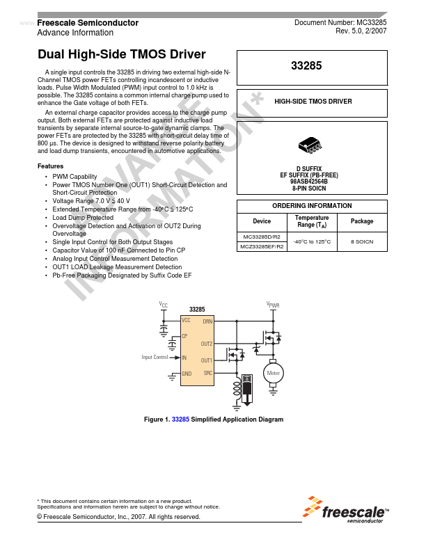
Datasheet4U Logo Datasheet4U.com

33285 - Dual High-Side TMOS Driver

Datasheet Summary

Description

The power FETs are turned ON by charging their gate capacities with a current flowing out of pins OUT1 and OUT2.

During PWM, the values of table below are guaranteed.

They are measured with 8.0 nF on OUT1 and 16 nF on OUT2.

Features

  • PWM Capability.
  • Power TMOS Number One (OUT1) Short-Circuit Detection and Short-Circuit Protection.
  • Voltage Range 7.0 V ≤ 40 V.
  • Extended Temperature Range from -40°C ≤ 125°C.
  • Load Dump Protected.
  • Overvoltage Detection and Activation of OUT2 During Overvoltage.
  • Single Input Control for Both Output Stages.
  • Capacitor Value of 100 nF Connected to Pin CP.
  • Analog Input Control Measurement Detection.
  • OUT1 LOAD Lea.

📥 Download Datasheet

Datasheet preview – 33285

Datasheet Details

Part number 33285
Manufacturer Freescale Semiconductor
File Size 338.44 KB
Description Dual High-Side TMOS Driver
Datasheet download datasheet 33285 Datasheet
Additional preview pages of the 33285 datasheet.
Other Datasheets by Freescale Semiconductor

Full PDF Text Transcription

Click to expand full text
www.DataSheet4U.com Freescale Semiconductor Advance Information Document Number: MC33285 Rev. 5.0, 2/2007 Dual High-Side TMOS Driver A single input controls the 33285 in driving two external high-side NChannel TMOS power FETs controlling incandescent or inductive loads. Pulse Width Modulated (PWM) input control to 1.0 kHz is possible. The 33285 contains a common internal charge pump used to enhance the Gate voltage of both FETs. An external charge capacitor provides access to the charge pump output. Both external FETs are protected against inductive load transients by separate internal source-to-gate dynamic clamps. The power FETs are protected by the 33285 with short-circuit delay time of 800 µs.
Published: |