MCZ33742
MCZ33742 is System Basis Chip manufactured by Freescale Semiconductor.
Features
- 1.0 Mbps CAN Transceiver Bus Interface with Bus Diagnostic Capability
- SPI Control at Frequencies up to 4.0 Mhz
- 5.0 V Low Dropout Voltage Regulator with Current Limiting, Overtemperature Pre-Warning, and Output Monitoring and Reset
- A Second 5.0 V Regulator Capability using an External Series Pass Transistor
- Normal, Standby, Stop, and Sleep Modes of Operation with Low Sleep and Stop Mode Current
- A High-Side (HS) Switch Output Driver for Controlling External Circuitry.
- Pb-Free Packaging Designated by Suffix Code EG and EP
33742 33742S
SYSTEM BASIS CHIP
DW SUFFIX EG SUFFIX (PB-FREE) 98ASB42345B 28-PIN SOICW
EP SUFFIX (PB-FREE) 98ARH99048A 48-PIN QFN
ORDERING INFORMATION
Device MC33742DW/R2 MCZ33742EG/R2 MC33742SDW/R2 MCZ33742SEG/R2 PCZ33742EP/R2 48 QFN
- 40°C to 125°C 28 SOICW Temperature Range (TA) Package
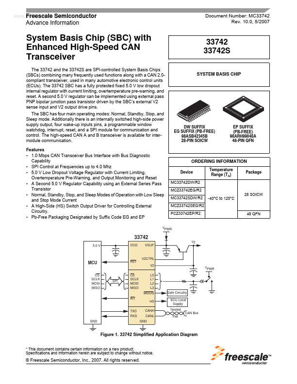
VPWR
5.0 V VDD VSUP V2CTRL V2 L0 L1 L2 L3 WDOG HS CANH CANL GND
V2
MCU CS SCLK MOSI MISO
RST CS SCLK MOSI MISO INT TXD RXD
VPWR
Safe Circuitry ECU Local Supply Twisted CAN Bus Pair
Figure 1. 33742 Simplified Application Diagram
- This document contains certain information on a new product. Specifications and information herein are subject to change without notice.
© Freescale Semiconductor, Inc., 2007. All rights reserved.
DEVICE VARIATIONS
DEVICE VARIATIONS
Table 1. Device Differences During a Reset Condition
Part No. 33742 Reset Duration 15 ms (typical) Device Differences The duration the RST pin is asserted low when the Reset mode is entered after the SBC is powered up and a VDD undervoltage condition is detected and the watchdog register is not properly triggered. The duration the RST pin is asserted low when the Reset mode is entered after the SBC is powered up and a VDD undervoltage condition is detected and the watchdog register is not properly triggered. See Page page 19
33742S
3.5 ms (typical) page 19
Analog Integrated Circuit...