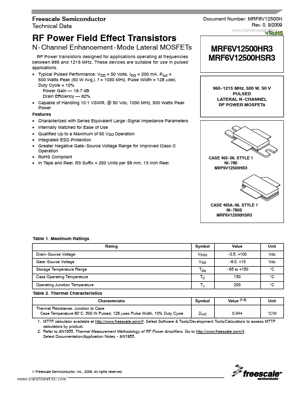
Datasheet4U Logo Datasheet4U.com

MRF6V12500HSR3 - RF Power Field Effect Transistors

Download the MRF6V12500HSR3 datasheet PDF. This datasheet also covers the MRF6V12500HR3 variant, as both devices belong to the same rf power field effect transistors family and are provided as variant models within a single manufacturer datasheet.

General Description

5.1 pF Chip Capacitors 33 pF Chip Capacitors 10 μF, 50 V Chip Capacitors 2.2 μF, 100 V Chip Capacitors 22 μF, 25 V Chip Capacitor 1 μF, 100 V Chip Capacitor 470 μF, 63 V Electrolytic Capacitors 56 Ω, 1/4 W Chip Resistors 0 Ω, 3 A Chip Resistors Part Number ATC100B5R1CT500XT ATC100B330JT500XT GRM55DR

Key Features

  • Characterized with Series Equivalent Large - Signal Impedance Parameters.
  • Internally Matched for Ease of Use.
  • Qualified Up to a Maximum of 50 VDD Operation.
  • Integrated ESD Protection.
  • Greater Negative Gate - Source Voltage Range for Improved Class C Operation.
  • RoHS Compliant.
  • In Tape and Reel. R3 Suffix = 250 Units per 56 mm, 13 inch Reel. MRF6V12500HR3 MRF6V12500HSR3 965 - 1215 MHz, 500 W, 50 V PULSED.

📥 Download Datasheet

Note: The manufacturer provides a single datasheet file (MRF6V12500HR3_FreescaleSemiconductor.pdf) that lists specifications for multiple related part numbers.

Full PDF Text Transcription (Reference)

The following content is an automatically extracted verbatim text from the original manufacturer datasheet and is provided for reference purposes only.

View original datasheet text
Freescale Semiconductor Technical Data Document Number: MRF6V12500H Rev. 0, 9/2009 www.DataSheet4U.com RF Power Field Effect Transistors N - Channel Enhancement - Mode Lateral MOSFETs RF Power transistors designed for applications operating at frequencies between 965 and 1215 MHz. These devices are suitable for use in pulsed applications. • Typical Pulsed Performance: VDD = 50 Volts, IDQ = 200 mA, Pout = 500 Watts Peak (50 W Avg.), f = 1030 MHz, Pulse Width = 128 μsec, Duty Cycle = 10% Power Gain — 19.