MRFG35010
MRFG35010 is Gallium Arsenide PHEMT RF Power Field Effect Transistor manufactured by Freescale Semiconductor.
..
Freescale Semiconductor Technical Data
MRFG35010 Rev. 6, 12/2004
Gallium Arsenide PHEMT
RF Power Field Effect Transistor
Designed for WLL/MMDS or UMTS driver applications with frequencies from 1.8 to 3.6 GHz. Device is unmatched and is suitable for use in Class AB or Class A linear base station applications.
- Typical W- CDMA Performance:
- 42 d Bc ACPR, 3.55 GHz, 12 Volts, IDQ = 180 m A, 5 MHz Offset/3.84 MHz BW, 64 DPCH (8.5 d B P/A @ 0.01% Probability) Output Power
- 1 Watt Power Gain
- 10 d B Efficiency
- 30%
- 10 Watts P1d B @ 3.55 GHz
- Excellent Phase Linearity and Group Delay Characteristics
- High Gain, High Efficiency and High Linearity
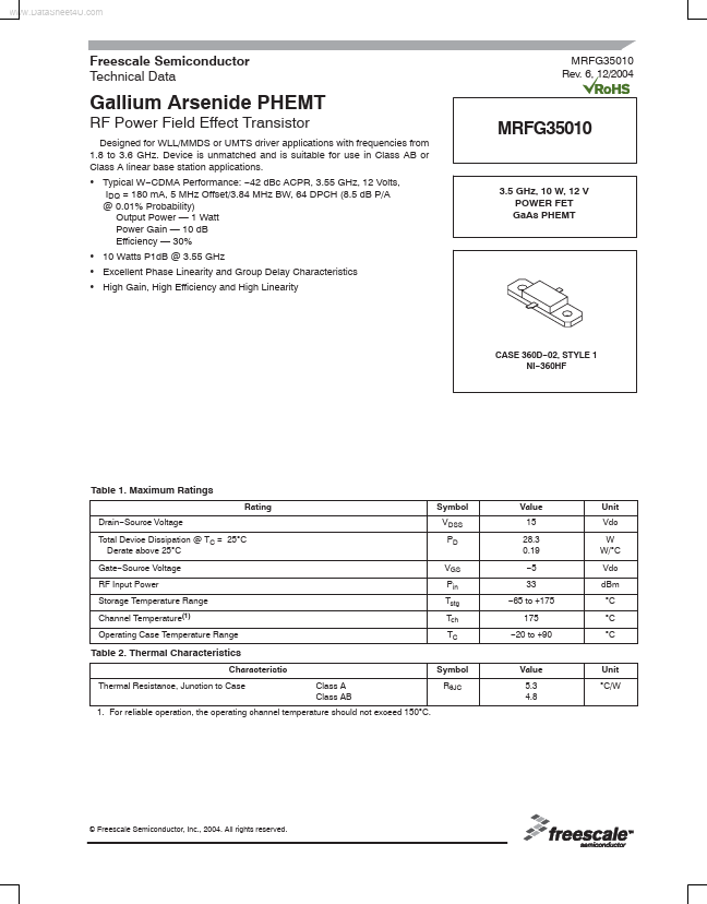
3.5 GHz, 10 W, 12 V POWER FET Ga As PHEMT
CASE 360D- 02, STYLE 1 NI- 360HF
Table 1. Maximum Ratings
Rating Drain- Source Voltage Total Device Dissipation @ TC = 25°C Derate above 25°C Gate- Source Voltage RF Input Power Storage Temperature Range Channel Temperature(1) Symbol VDSS PD VGS Pin Tstg Tch TC Value 15 28.3 0.19
- 5 33
- 65 to +175 175
- 20 to +90 Unit Vdc W W/°C Vdc d Bm °C °C °C
Operating Case Temperature Range
Table 2. Thermal Characteristics
Characteristic Thermal Resistance, Junction to Case Class A Class AB Symbol RθJC Value 5.3 4.8 Unit °C/W
1. For reliable operation, the operating channel temperature should not exceed 150°C.
© Freescale Semiconductor, Inc., 2004. All rights reserved.
MRFG35010 5- 1
Freescale Semiconductor Wireless RF Product Device Data
Table 3. Electrical Characteristics (TC = 25°C unless otherwise noted)
Characteristic Saturated Drain Current (VDS = 3.5 Vdc, VGS = 0 Vdc) Off State Leakage Current (VGS =
- 0.4 Vdc, VDS = 0 Vdc) Off State Drain Current (VDS = 12 Vdc, VGS =
- 1.9 Vdc) Off State Current (VDS = 28.5 Vdc, VGS =
- 2.5 Vdc) Gate- Source Cut- off Voltage (VDS = 3.5 Vdc, IDS = 15 m A) Quiescent Gate Voltage (VDS = 12 Vdc, ID = 180 m A) Power Gain (VDD = 12 Vdc, IDQ = 180 m A, f = 3.55 GHz) Output Power, 1 d B pression Point (VDD = 12 Vdc, IDQ = 180 m A, f = 3.55 GHz) Drain...