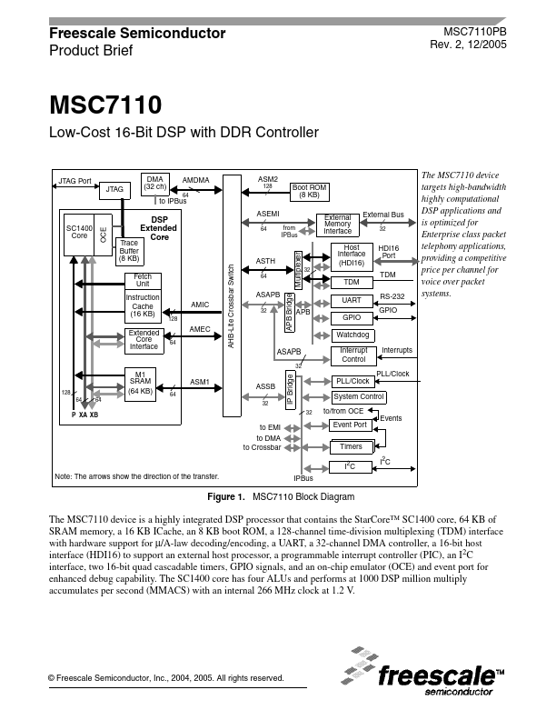
MSC7110
Features
Features
Table 1 lists the features of the Freescale MSC7110 device.
Table 1. MSC7110 Features
Feature
Description
- Up to 1000 MMACS using an internal 266 MHz clock at 1.2 V. A multiply-accumulate operation includes a multiply-add instruction with the associated data move and pointer update.
- 4 data ALUs.
- 16 data registers, 40 bits each.
- 27 address registers, 32 bits each.
- Hardware support for fractional and integer data types.
- Very rich 16-bit wide orthogonal instruction set.
- Up to six instructions executed in a single clock cycle.
- Variable-length execution set (VLES) that can be optimized for code density and performance.
- JTAG port designed to ply with IEEE® Std 1149.1™.
- On-chip emulator (OCE) module with real-time debugging capabilities. The high performance extended core delivers up to 1000 MMACS using 4 ALUs running up to 266 MHz, including:
- SC1400 core processor.
- 64 KB multi-port SRAM (M1) accessed by the SC1400 core with no wait states.
- 16 KB,...