Datasheet4U Logo Datasheet4U.com

MW7IC18100NBR1 - RF LDMOS Wideband Integrated Power Amplifiers

Download the MW7IC18100NBR1 datasheet PDF. This datasheet also covers the MW7IC18100GNR1 variant, as both devices belong to the same rf ldmos wideband integrated power amplifiers family and are provided as variant models within a single manufacturer datasheet.

General Description

6.8 pF Chip Capacitors 10 μF, 50 V Chip Capacitors 0.2 pF Chip Capacitors 0.5 pF Chip Capacitors 0.8 pF Chip Capacitor 1.5 pF Chip Capacitor 2.2 μF, 16 V Chip Capacitor 470 μF, 63 V Electrolytic Capacitor, Radial 10 KΩ, 1/4 W Chip Resistors Part Number ATC100B6R8BT500XT GRM55DR61H106KA88L ATC100B0R2

Key Features

  • Characterized with Series Equivalent Large - Signal Impedance Parameters and Common Source Scattering Parameters.
  • On - Chip Matching (50 Ohm Input, DC Blocked).
  • Integrated Quiescent Current Temperature Compensation with Enable/Disable Function (1).
  • Integrated ESD Protection.
  • 200°C Capable Plastic Package.
  • RoHS Compliant.
  • In Tape and Reel. R1 Suffix = 500 Units per 44 mm, 13 inch Reel
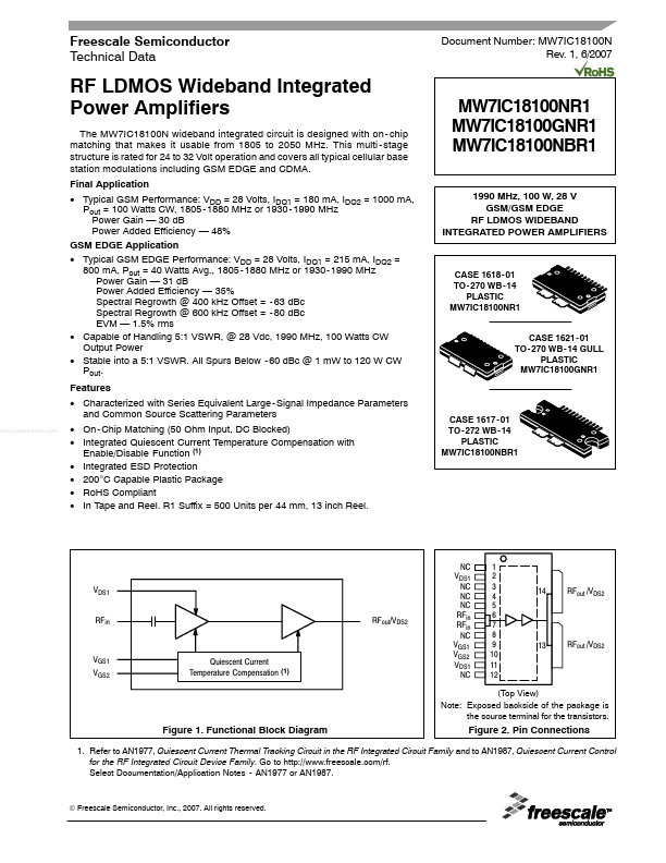
. MW7IC18100NR1 MW7IC18100GNR1 MW7IC18100NBR1 199.

📥 Download Datasheet

Note: The manufacturer provides a single datasheet file (MW7IC18100GNR1_FreescaleSemiconductor.pdf) that lists specifications for multiple related part numbers.

Full PDF Text Transcription (Reference)

The following content is an automatically extracted verbatim text from the original manufacturer datasheet and is provided for reference purposes only.

View original datasheet text
Freescale Semiconductor Technical Data Document Number: MW7IC18100N Rev. 1, 6/2007 RF LDMOS Wideband Integrated Power Amplifiers The MW7IC18100N wideband integrated circuit is designed with on - chip matching that makes it usable from 1805 to 2050 MHz. This multi - stage structure is rated for 24 to 32 Volt operation and covers all typical cellular base station modulations including GSM EDGE and CDMA. Final Application • Typical GSM Performance: VDD = 28 Volts, IDQ1 = 180 mA, IDQ2 = 1000 mA, Pout = 100 Watts CW, 1805 - 1880 MHz or 1930 - 1990 MHz Power Gain — 30 dB Power Added Efficiency — 48% GSM EDGE Application • Typical GSM EDGE Performance: VDD = 28 Volts, IDQ1 = 215 mA, IDQ2 = 800 mA, Pout = 40 Watts Avg.