AOD3N50 Overview
Key Specifications
Package: TO-252
Mount Type: Surface Mount
Max Operating Temp: 150 °C
Min Operating Temp: -50 °C
Description
The AOD3N50 & AOU3N50 have been fabricated using an advanced high voltage MOSFET process that is designed to deliver high levels of performance and robustness in popular AC-DC applications. By providing low RDS(on), Ciss and Crss along with guaranteed avalanche capability these parts can be adopted quickly into new and existing offline power supply designs.
Key Features
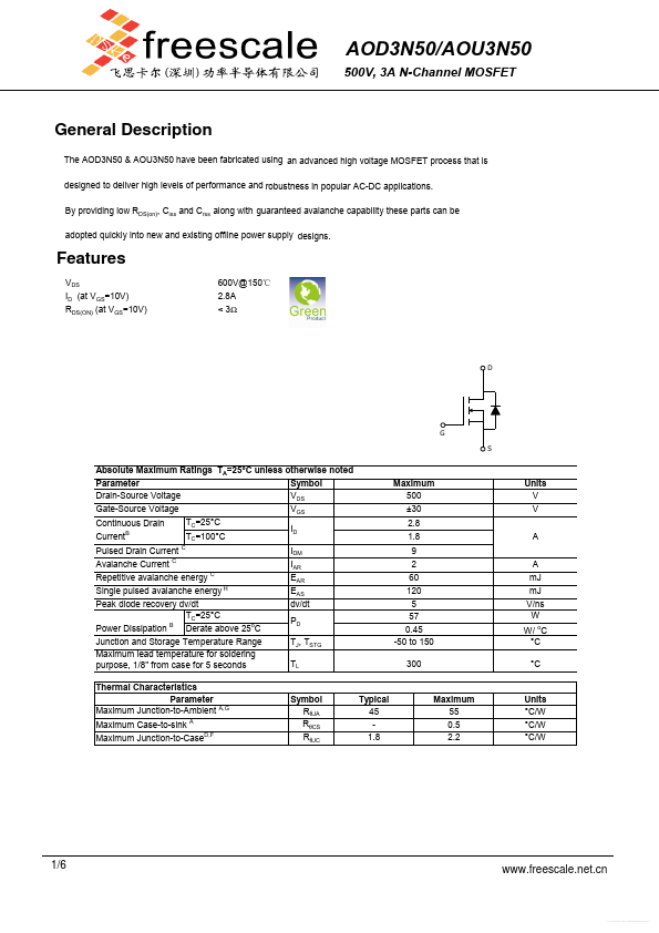
- VDS ID (at VGS=10V) RDS(ON) (at VGS=10V) 600V@150℃ 2.8A < 3Ω D G S