2SK3776-01
2SK3776-01 is N-CHANNEL SILICON POWER MOSFET manufactured by Fuji Electric.
Features
High speed switching, Low on-resistance Low driving power, Avalanche-proof No secondary breakdown
Applications
Switching regulators UPS (Uninterruptible Power Supply) DC-DC converters
Maximum ratings and characteristic
Absolute maximum ratings (Tc=25°C unless otherwise specified)
Item Drain-source voltage Continuous Drain Current Pulsed Drain Current Gate-Source Voltage Maximum Avalanche current Non-Repetitive Maximum Avalanche Energy Repetitive Maximum Avalanche Energy Maximum Drain-Source d V/dt Peak Diode Recovery d V/dt Max. Power Dissipation Operating and Storage Temperature range Symbol V DS VDSX ID ID(puls] VGS IAR EAS EAR d V DS /dt d V/dt PD Tch Tstg Ratings 300 300 53 ±212 ±30 53 1013.9 41 20 5 410 2.50 +150 -55 to +150 Unit V V A A V A m J m J Remarks VGS=-30V
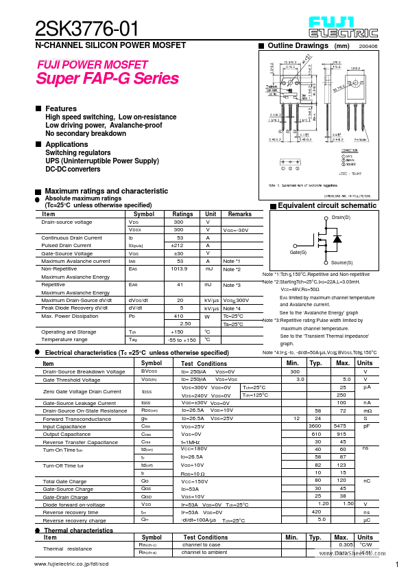
Equivalent circuit schematic
Drain(D)
Gate(G)
Note
- 1 Note
- 2 Note
- 3
Source(S) Note
- 1:Tch < = 150°C,Repetitive and Non-repetitive Note
- 2:Starting Tch=25°C,IAS=22A,L=3.03m H, VCC=48V,RG=50Ω EAS limited by maximum channel temperature and Avalanche current. See to the ‘Avalanche Energy’ graph Note
- 3:Repetitive rating:Pulse width limited by maximum channel temperature. See to the ‘Transient Thermal impedance’ graph. k V/µs VDS= < 300V k V/µs Note
- 4 Tc=25°C W Ta=25°C °C °C
Electrical characteristics (Tc =25°C unless otherwise specified)
Item Drain-Source Breakdown Voltage Gate Threshold Voltage Zero Gate Voltage Drain Current Gate-Source Leakage Current Drain-Source On-State Resistance Forward Transconductance Input Capacitance Output Capacitance Reverse Transfer Capacitance Turn-On Time ton Turn-Off Time toff Total Gate Charge Gate-Source Charge Gate-Drain Charge Diode forward on-voltage Reverse recovery time Reverse recovery charge Symbol BVDSS VGS(th) IDSS IGSS RDS(on) gfs Ciss Coss Crss td(on) tr td(off) tf QG QGS QGD V SD trr Qrr Symbol Rth(ch-c) Rth(ch-a)
< Note
- 4:IF < = BVDSS,Tch< = -ID, -di/dt=50A/µs,VCC = 150°C
Test Conditions ID= 250µA VGS=0V ID= 250µA VDS=VGS Tch=25°C VDS =300V...