Datasheet4U Logo Datasheet4U.com

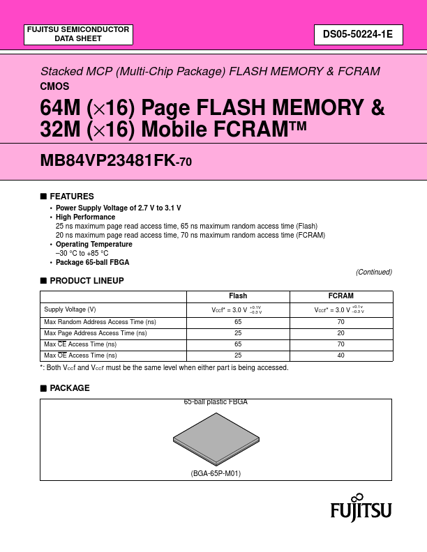
MB84VP23481FK-70 - 64M (X16) Page FLASH MEMORY & 32M (X16) Mobile FCRAMTM

General Description

Pin name A20 to A0 A21 DQ15 to DQ0 CEf CE1r CE2r OE WE RY/BY UB LB RESET WP/ACC N.C.

Power Power Power Address Inputs (Common) Address Input (Flash) Data Inputs/Outputs (Common) Chip Enable (Flash) Chip Enable (FCRAM) Chip Enable (FCR

Key Features

  • Power Supply Voltage of 2.7 V to 3.1 V.
  • High Performance 25 ns maximum page read access time, 65 ns maximum random access time (Flash) 20 ns maximum page read access time, 70 ns maximum random access time (FCRAM).
  • Operating Temperature.
  • 30 °C to +85 °C.
  • Package 65-ball FBGA (Continued) s.

📥 Download Datasheet

Full PDF Text Transcription (Reference)

The following content is an automatically extracted verbatim text from the original manufacturer datasheet and is provided for reference purposes only.

View original datasheet text
www.DataSheet4U.com FUJITSU SEMICONDUCTOR DATA SHEET DS05-50224-1E Stacked MCP (Multi-Chip Package) FLASH MEMORY & FCRAM CMOS 64M (×16) Page FLASH MEMORY & 32M (×16) Mobile FCRAMTM MB84VP23481FK-70 s FEATURES • Power Supply Voltage of 2.7 V to 3.1 V • High Performance 25 ns maximum page read access time, 65 ns maximum random access time (Flash) 20 ns maximum page read access time, 70 ns maximum random access time (FCRAM) • Operating Temperature –30 °C to +85 °C • Package 65-ball FBGA (Continued) s PRODUCT LINEUP Flash Supply Voltage (V) Max Random Address Access Time (ns) Max Page Address Access Time (ns) Max CE Access Time (ns) Max OE Access Time (ns) VCCf* = 3.0 V 65 25 65 25 +0.1V –0.3 V FCRAM VCCr* = 3.0 V –0.3 V 70 20 70 40 +0.