MBM29DL161BD
MBM29DL161BD is FLASH MEMORY CMOS 16M (2M X 8/1M X 16) BIT manufactured by Fujitsu Semiconductor Limited.
- Part of the MBM29DL16xTD comparator family.
- Part of the MBM29DL16xTD comparator family.
FEATURES
Dual Operation
- 0.33 µm Process Technology
- Simultaneous Read/Write operations (dual bank) Multiple devices available with different bank sizes (Refer to “MBM29DL16XTD/BD Device Bank Divisions Table” in s GENERAL DESCRIPTION
) Host system can program or erase in one bank, then immediately and simultaneously read from the other bank Zero latency between read and write operations Read-while-erase Read-while-program
- Single 3.0 V read, program, and erase Minimizes system level power requirements (Continued) s PRODUCT LINE UP
Part No. Ordering Part No. VCC = 3.3 V VCC = 3.0 V
+0.3 V
- 0.3 V +0.6 V
- 0.3 V
MBM29DL16XTD/MBM29DL16XBD 70
- 70 70 30
- 90 90 90 35
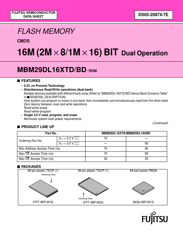
Max Address Access Time (ns) Max CE Access Time (ns) Max OE Access Time (ns) s PACKAGES
48-pin plastic TSOP (1)
Marking Side
48-pin plastic TSOP (1)
48-ball plastic FBGA
Marking Side
(FPT-48P-M19)
(FPT-48P-M20)
(BGA-48P-M13)
MBM29DL16XTD/BD-70/90
(Continued)
- patible with JEDEC-standard mands Uses same software mands as E2PROMs
- patible with JEDEC-standard world-wide pinouts 48-pin TSOP(1) (Package suffix: PFTN
- Normal Bend Type, PFTR
- Reversed Bend Type) 48-ball FBGA (Package suffix: PBT)
- Minimum 100,000 program/erase cycles
- High performance 70 ns maximum access time
- Sector erase architecture Eight 4K word and thirty one 32K word sectors in word mode Eight 8K byte and thirty one 64K byte sectors in byte mode Any bination of sectors can be concurrently erased. Also supports full chip erase.
- Boot Code Sector Architecture T = Top sector B = Bottom sector
- Hidden ROM region 64K byte of Hidden ROM, accessible through a new “Hidden ROM Enable” mand sequence Factory serialized and protected to provide a secure electronic serial number (ESN)
- WP/ACC input pin At VIL, allows protection of boot sectors, regardless of sector group protection/unprotection status At VACC, increases program performance
- Embedded Erase TM- Algorithms Automatically pre-programs and erases the chip or any sector
-...