MBM29LV080A Overview
Key Features
- Address specification is not necessary during command sequence
- Single 3.0 V read, program and erase Minimizes system level power requirements
- Compatible with JEDEC-standard commands Uses same software commands as E2PROMs
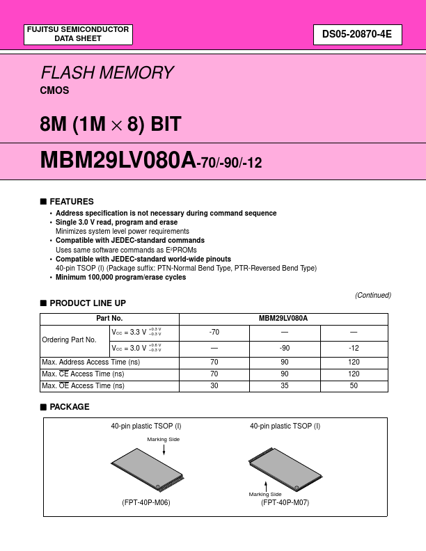
- Compatible with JEDEC-standard world-wide pinouts 40-pin TSOP (I) (Package suffix: PTN-Normal Bend Type, PTR-Reversed Bend Type)
- High performance 70 ns maximum access time
- Sector erase architecture 16 sectors of 64K bytes each Any combination of sectors can be concurrently erased. Also supports full chip erase
- Embedded EraseTM* Algorithms Automatically pre-programs and erases the chip or any sector
- Embedded programTM* Algorithms Automatically programs and verifies data at specified address
- Data Polling and Toggle Bit feature for detection of program or erase cycle completion
- Ready/Busy output (RY/BY) Hardware method for detection of program or erase cycle completion