Datasheet4U Logo Datasheet4U.com

MB8117-12 - NMOS Dynamic Random Access Memory

Download the MB8117-12 datasheet PDF. This datasheet also covers the MB8117-10 variant, as both devices belong to the same nmos dynamic random access memory family and are provided as variant models within a single manufacturer datasheet.

General Description

The Fujitsu MB8117 is a fully decoded, dynamic NMOS random access memory organized as 16,384 one-bit words.

Key Features

  • 16,384 x 1 RAM, 16 pin package e Silicon-gate, Double Poly NMOS single-transistor cell.
  • Address access time 100 ns max (MB8117-10) 120 ns max (MB8117-12).
  • Cycle time, 235 ns min (MB8117-10) 270 ns min (MB8117-12).
  • Low power: 182 mW max (MB8117-10) 160 mW max (MB8117-12) 19_5 mW max (Standby).
  • +5V single power supply, :t 10% tolerance.
  • On-chip substrate bias generator.
  • All Inputs TTL compatible, low capacitive load.
  • Thre. s.

📥 Download Datasheet

Note: The manufacturer provides a single datasheet file (MB8117-10-Fujitsu.pdf) that lists specifications for multiple related part numbers.

Full PDF Text Transcription (Reference)

The following content is an automatically extracted verbatim text from the original manufacturer datasheet and is provided for reference purposes only.

View original datasheet text
FUJITSU MICROELECTRONICS NMOS 16,384·BIT DYNAlVIIC RANDOM ACCESS :MEMORY DESCRIPTION The Fujitsu MB8117 is a fully decoded, dynamic NMOS random access memory organized as 16,384 one-bit words. The design is optimized for highspeed, high performance applications such as mainframe memory, buffer memory peripheral storage and environments where low power dissipation and compact layout are required. 
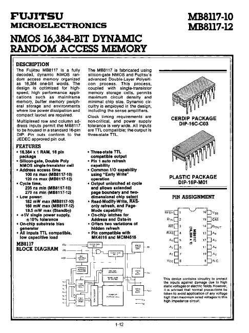
Multiplexed row and column address inputs permit the MB8117 to be housed in a standard 16-pin DIP. Pin outs conform to the JEDEC approved pin out. The MB8117 Is fabricated using silicon-gate NMOS and FUjitsu's advanced Double-Layer Polysilicon process. This process, coupled with single-transistor memory storage cells, permits maximum circuit density and minimal chip size.