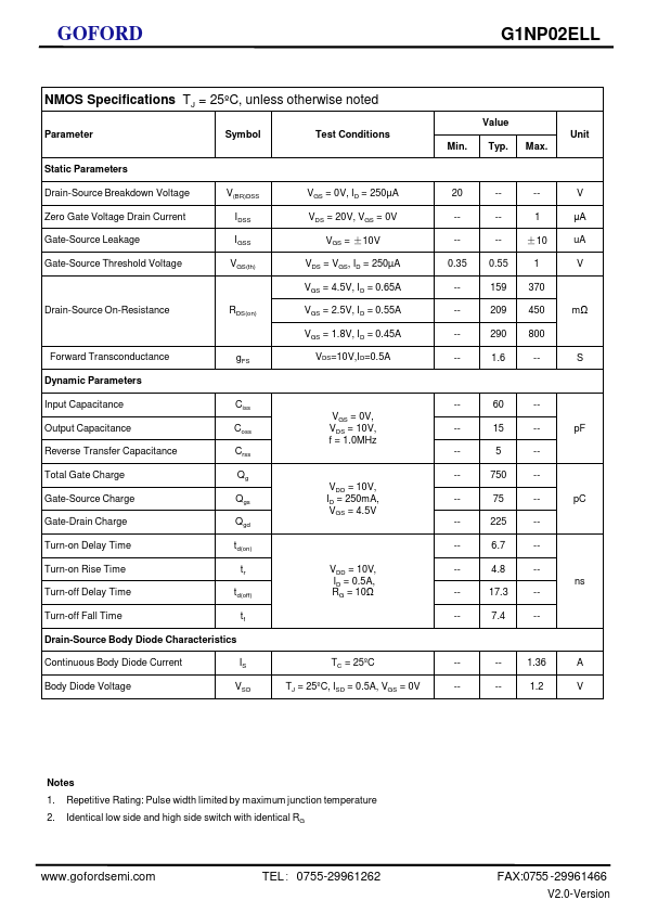
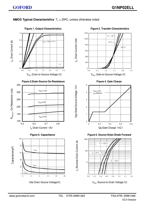
Datasheet4U Logo Datasheet4U.com

G1NP02 - N and P Channel Enhancement Mode Power MOSFET

Download the G1NP02 datasheet PDF. This datasheet also covers the G1NP02ELL variant, as both devices belong to the same n and p channel enhancement mode power mosfet family and are provided as variant models within a single manufacturer datasheet.

General Description

This Product uses advanced trench technology MOSFETs to provide excellent RDS(ON) and low gate charge.

The complementary MOSFETs may be used to form a level shifted high side switch, and for a host of other applications.

Key Features

  • NMOS.
  • VDS.
  • ID (at VGS = 10V).
  • RDS(ON) (at VGS = 4.5V).
  • RDS(ON) (at VGS = 2.5V).
  • RDS(ON) (at VGS = 1.8V) 20V 1.36A < 375mΩ < 450mΩ < 800mΩ.
  • PMOS.
  • VDS.
  • ID (at VGS = -10V).
  • RDS(ON) (at VGS = -4.5V).
  • RDS(ON) (at VGS = -2.5V).
  • RDS(ON) (at VGS = -1.8V).
  • 100% Avalanche Tested.
  • RoHS Compliant.
  • ESD (HBM)>2.0KV -20V -1.15A < 520mΩ < 700mΩ < 1000mΩ Schematic diagram Marking and pin assignment.

📥 Download Datasheet

Note: The manufacturer provides a single datasheet file (G1NP02ELL-GOFORD.pdf) that lists specifications for multiple related part numbers.

Datasheet Details

Part number G1NP02
Manufacturer GOFORD
File Size 554.33 KB
Description N and P Channel Enhancement Mode Power MOSFET
Datasheet download datasheet G1NP02 Datasheet

Full PDF Text Transcription (Reference)

The following content is an automatically extracted verbatim text from the original manufacturer datasheet and is provided for reference purposes only.

View original datasheet text
GOFORD N and P Channel Enhancement Mode Power MOSFET Description This Product uses advanced trench technology MOSFETs to provide excellent RDS(ON) and low gate charge. The complementary MOSFETs may be used to form a level shifted high side switch, and for a host of other applications. G1NP02ELL General Features ⚫ NMOS ⚫ VDS ⚫ ID (at VGS = 10V) ⚫ RDS(ON) (at VGS = 4.5V) ⚫ RDS(ON) (at VGS = 2.5V) ⚫ RDS(ON) (at VGS = 1.8V) 20V 1.36A < 375mΩ < 450mΩ < 800mΩ ⚫ PMOS ⚫ VDS ⚫ ID (at VGS = -10V) ⚫ RDS(ON) (at VGS = -4.5V) ⚫ RDS(ON) (at VGS = -2.5V) ⚫ RDS(ON) (at VGS = -1.8V) ⚫ 100% Avalanche Tested ⚫ RoHS Compliant ⚫ ESD (HBM)>2.0KV -20V -1.