SSS1206
SSS1206 is N-Channel MOSFET manufactured by Good-Ark Semiconductor.
- Part of the SSS1206-GOOD comparator family.
- Part of the SSS1206-GOOD comparator family.
Features and Benefits
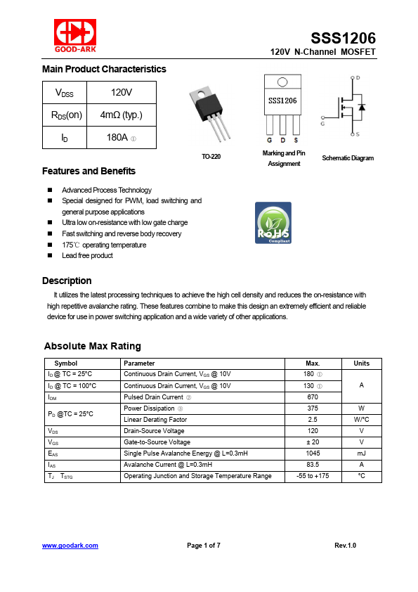
TO-220
- Advanced Process Technology
- Special designed for PWM, load switching and general purpose applications
- Ultra low on-resistance with low gate charge
- Fast switching and reverse body recovery
- 175℃ operating temperature
- Lead free product
120V N-Channel MOSFET
Marking and Pin Assignment
Schematic Diagram
Description
It utilizes the latest processing techniques to achieve the high cell density and reduces the on-resistance with high repetitive avalanche rating. These features bine to make this design an extremely efficient and reliable device for use in power switching application and a wide variety of other applications.
Absolute Max Rating
Symbol ID @ TC = 25°C ID @ TC = 100°C IDM
PD @TC = 25°C
VDS VGS EAS IAS TJ TSTG
Parameter Continuous Drain Current, VGS @ 10V Continuous Drain Current, VGS @ 10V Pulsed Drain Current ② Power Dissipation ③ Linear Derating Factor Drain-Source Voltage Gate-to-Source Voltage Single Pulse Avalanche Energy @ L=0.3m H Avalanche Current @ L=0.3m H Operating Junction and Storage Temperature Range
Max. 180 ① 130 ①
670 375 2.5 120 ± 20 1045 83.5 -55 to +175
Units
W W/°C
V V m J A °C
.goodark.
Page 1 of 7
Rev.1.0
120V N-Channel MOSFET
Thermal Resistance
Symbol RθJC
RθJA
Characteristics Junction-to-case ③ Junction-to-ambient (t ≤ 10s) ④ Junction-to-Ambient (PCB mounted, steady-state) ④
Typ.
- -
- Max. 0.4 62 40
Units °C/W °C/W °C/W
Electrical Characteristics @TA=25℃ unless otherwise specified
Symbol Parameter V(BR)DSS Drain-to-Source breakdown voltage
RDS(on) Static Drain-to-Source on-resistance
VGS(th) Gate threshold...