Datasheet4U Logo Datasheet4U.com

GS81313LT36GK - 144Mb SigmaDDR-IIIe Burst of 2 ECCRAM

Download the GS81313LT36GK datasheet PDF. This datasheet also covers the GS81313LT18GK-833 variant, as both devices belong to the same 144mb sigmaddr-iiie burst of 2 eccram family and are provided as variant models within a single manufacturer datasheet.

Description

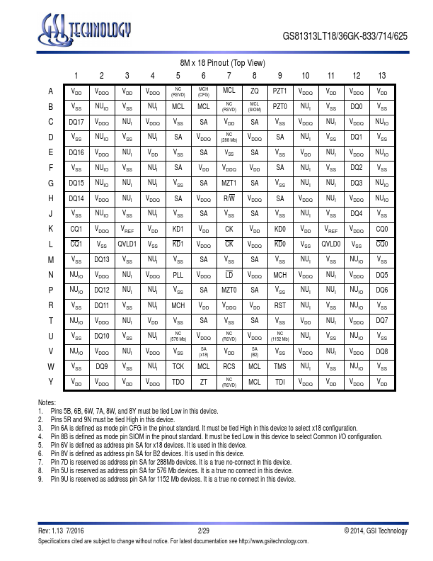
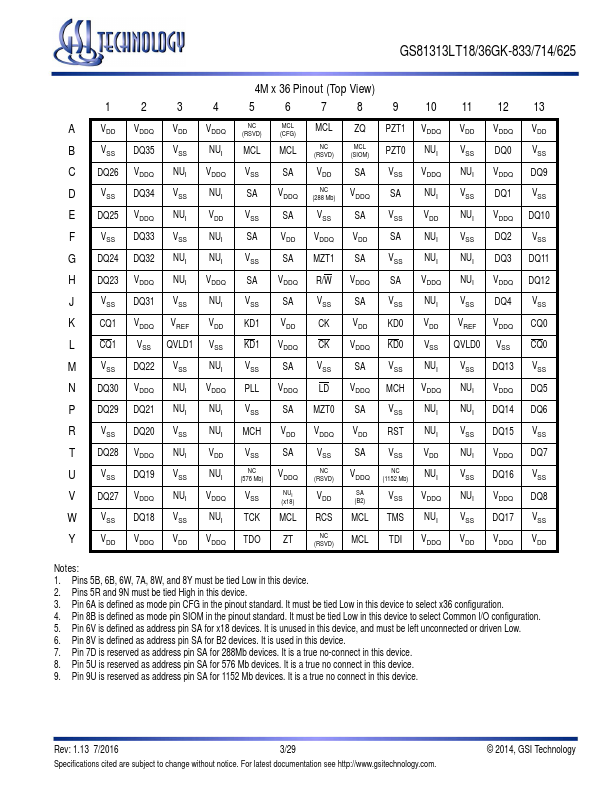
Symbol Description SA DQ[35:0] QVLD[1:0] CK, CK KD[1:0], KD[1:0] CQ[1:0], CQ[1:0] LD R/W PLL RST ZQ ZT RCS MZT[1:0] Address

Read or Write Address is registered on CK.

Registered on KD and KD during Write operations; aligned with CQ and CQ during Read oper

Features

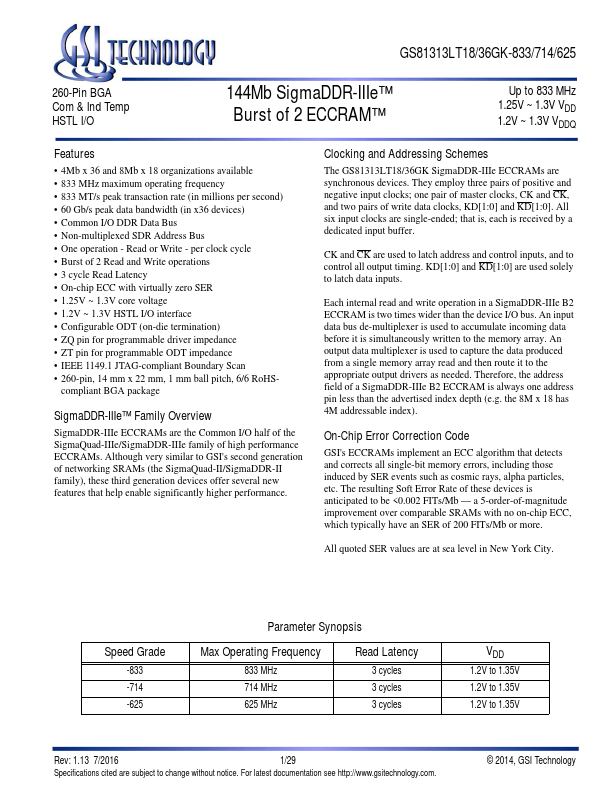
  • 4Mb x 36 and 8Mb x 18 organizations available.
  • 833 MHz maximum operating frequency.
  • 833 MT/s peak transaction rate (in millions per second).
  • 60 Gb/s peak data bandwidth (in x36 devices).
  • Common I/O DDR Data Bus.
  • Non-multiplexed SDR Address Bus.
  • One operation - Read or Write - per clock cycle.
  • Burst of 2 Read and Write operations.
  • 3 cycle Read Latency.
  • On-chip ECC with virtually zero SER.
  • 1.25V ~ 1.

📥 Download Datasheet

Note: The manufacturer provides a single datasheet file (GS81313LT18GK-833-GSITechnology.pdf) that lists specifications for multiple related part numbers.

Datasheet Details

Part number GS81313LT36GK
Manufacturer GSI Technology
File Size 204.63 KB
Description 144Mb SigmaDDR-IIIe Burst of 2 ECCRAM
Datasheet download datasheet GS81313LT36GK Datasheet

Full PDF Text Transcription

Click to expand full text
GS81313LT18/36GK-833/714/625 260-Pin BGA Com & Ind Temp HSTL I/O 144Mb SigmaDDR-IIIe™ Burst of 2 ECCRAM™ Up to 833 MHz 1.25V ~ 1.3V VDD 1.2V ~ 1.3V VDDQ Features • 4Mb x 36 and 8Mb x 18 organizations available • 833 MHz maximum operating frequency • 833 MT/s peak transaction rate (in millions per second) • 60 Gb/s peak data bandwidth (in x36 devices) • Common I/O DDR Data Bus • Non-multiplexed SDR Address Bus • One operation - Read or Write - per clock cycle • Burst of 2 Read and Write operations • 3 cycle Read Latency • On-chip ECC with virtually zero SER • 1.25V ~ 1.3V core voltage • 1.2V ~ 1.3V HSTL I/O interface • Configurable ODT (on-die termination) • ZQ pin for programmable driver impedance • ZT pin for programmable ODT impedance • IEEE 1149.
Published: |