GS8161E32B
GS8161E32B is Sync Burst SRAMs manufactured by GSI Technology.
- Part of the GS8161E18B comparator family.
- Part of the GS8161E18B comparator family.
GS8161E18B(T/D)/GS8161E32B(D)/GS8161E36B(T/D)
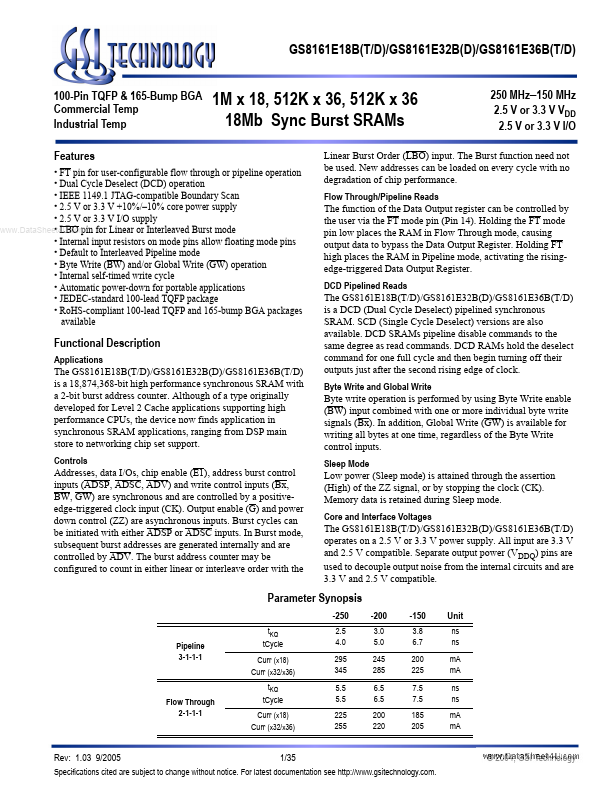
100-Pin TQFP & 165-Bump BGA mercial Temp Industrial Temp Features
- FT pin for user-configurable flow through or pipeline operation
- Dual Cycle Deselect (DCD) operation
- IEEE 1149.1 JTAG-patible Boundary Scan
- 2.5 V or 3.3 V +10%/- 10% core power supply
- 2.5 V or 3.3 V I/O supply ..
- LBO pin for Linear or Interleaved Burst mode
- Internal input resistors on mode pins allow floating mode pins
- Default to Interleaved Pipeline mode
- Byte Write (BW) and/or Global Write (GW) operation
- Internal self-timed write cycle
- Automatic power-down for portable applications
- JEDEC-standard 100-lead TQFP package
- RoHS-pliant...