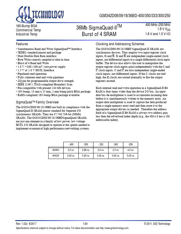
Full PDF Text Transcription for GS8342D08BD (Reference)
Note: Below is a high-fidelity text extraction (approx. 800 characters) for
GS8342D08BD. For precise diagrams, and layout, please refer to the original PDF.
GS8342D08/09/18/36BD-400/350/333/300/250 165-Bump BGA Commercial Temp Industrial Temp 36Mb SigmaQuad-IITM Burst of 4 SRAM 400 MHz–250 MHz 1.8 V VDD 1.8 V and 1.5 V I/O Fe...
View more extracted text
-IITM Burst of 4 SRAM 400 MHz–250 MHz 1.8 V VDD 1.8 V and 1.5 V I/O Features • Simultaneous Read and Write SigmaQuad™ Interface • JEDEC-standard pinout and package • Dual Double Data Rate interface • Byte Write controls sampled at data-in time • Burst of 4 Read and Write • 1.8 V +100/–100 mV core power supply • 1.5 V or 1.8 V HSTL Interface • Pipelined read operation • Fully coherent read and write pipelines • ZQ pin for programmable output drive strength • IEEE 1149.