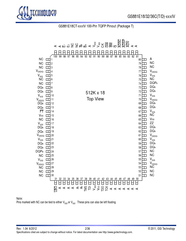
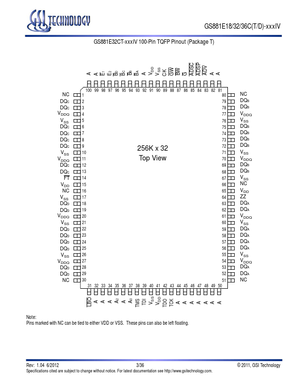
GS881E32CT-xxxIV Overview
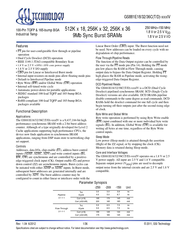
GS881E18/32/36C(T/D)-xxxIV 100-Pin TQFP & 165-bump BGA 512K x 18, 256K x 32, 256K x 36 Industrial Temp 9Mb Sync Burst SRAMs 250 MHz 150 MHz 1.8 V or 2.5 V VDD 1.8 V or 2.5.
GS881E32CT-xxxIV Key Features
- FT pin for user-configurable flow through or pipeline operation
- Dual Cycle Deselect (DCD) operation
- IEEE 1149.1 JTAG-patible Boundary Scan
- 1.8 V or 2.5 V +10%/-10% core power supply
- 1.8 V or 2.5 V I/O supply
- LBO pin for Linear or Interleaved Burst mode
- Internal input resistors on mode pins allow floating mode pins high places the RAM in Pipeline


