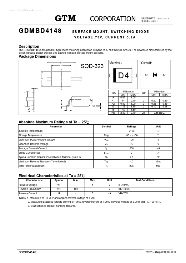
DESCRIPTION
S U R F A C E M O U N T, S W I T C H I N G D I O D E V O LT A G E 7 5 V, C U R R E N T 0 . 2 A Package Dimensions REF. A A1 A2 D E HE Millimeter Min. Max. 0.85 1.05 0 0.10 0.80 1.00 1.15 1.45 1.60 1.80 2.30 2.70 REF. L b c Q1 Millimeter Min. Max. 0.20 0.25 0.10 0.40 0.40 0.18 0.15 BSC. ABSOLUTE MAXIMUM RATINGS
at Ta = 25 Parameter Junction Temperature Storage Temperature Maximum Peak Reverse Voltage Maximum Reverse Voltage Average Forward Current Surge Current(1us) Typical Junction Capacitance between Terminal (Note 1) Maximum Reverse Recovery Time (Note2) Total Power Dissipation Symbol Tj Tstg VRM VR IO IFSM CJ TRR PD Ratings +150 -65 ~ +150 100 75 200 2 4.0 4.0 225 V V mA A pF nSec mW Unit ELECTRICAL CHARACTERISTICS
at Ta = 25 Characteristic Forward Voltage Reverse Breakdown Reverse Current Symbol VF VR IR Min. 100 Max. 1 5 Unit V V uA IF=10mA IR=100uA VR=75V . Test Conditions Notes: 1. Measured at 1.0 MHz and applied reverse voltage of 0 volt. 2. Measured at applied forward current of 10mA, reverse current of 1.0mA, Reverse voltage of 6.0volt and RL=100 3. GTM