GE90N03
GE90N03 is N-CHANNEL ENHANCEMENT MODE POWER MOSFET manufactured by GTM.
Description
Features
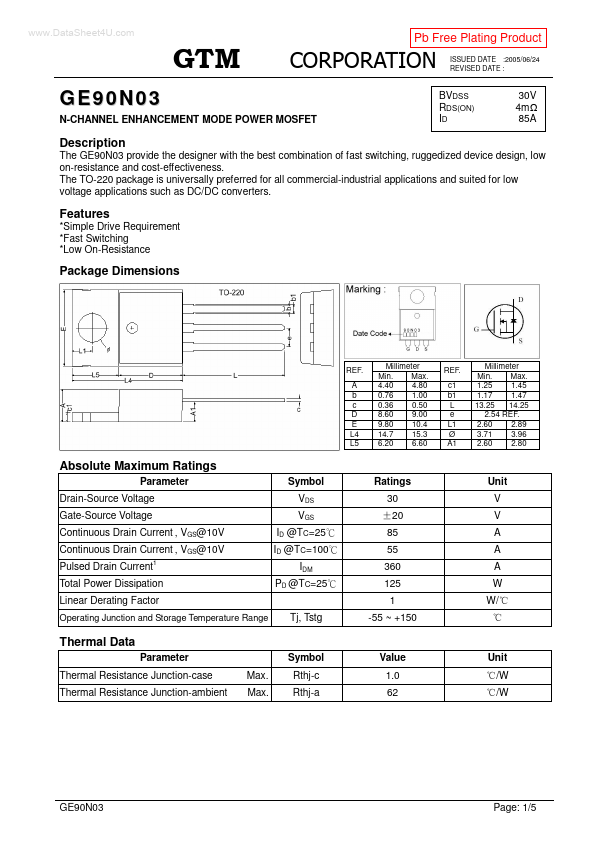
Package Dimensions
REF. A b c D E L4 L5
Millimeter Min. Max. 4.40 4.80 0.76 1.00 0.36 0.50 8.60 9.00 9.80 10.4 14.7 15.3 6.20 6.60
REF. c1 b1 L e L1 Ø A1
Millimeter Min. Max. 1.25 1.45 1.17 1.47 13.25 14.25 2.54 REF. 2.60 2.89 3.71 3.96 2.60 2.80
Absolute Maximum Ratings
Parameter Drain-Source Voltage Gate-Source Voltage Continuous Drain Current , VGS@10V Continuous Drain Current , VGS@10V Pulsed Drain Current
Symbol VDS VGS ID @TC=25 ID @TC=100 IDM PD @TC=25 Tj, Tstg
Ratings 30 20 85 55 360 125 1 -55 ~ +150
Unit V V A A A W W/
Total Power Dissipation Linear Derating Factor
Operating Junction and Storage Temperature Range
Thermal Data
Parameter Thermal Resistance Junction-case Thermal Resistance Junction-ambient Max. Max. Symbol Rthj-c Rthj-a Value 1.0 62 Unit /W /W
Page: 1/5
ISSUED DATE :2005/06/24 REVISED DATE :
Electrical Characteristics(Tj = 25
Parameter Drain-Source Breakdown Voltage
Breakdown Voltage Temperature Coefficient
Unless otherwise specified)
Min. 30 1.0 Typ. 0.035 90 3.2 4.5 100 10.5 60 14 115 95 180 3830 1900 850 Max. 3.0 100 1 25 4 5 p F ns n C Unit V V/ V S n A u A u A m Test Conditions VGS=0, ID=250u A Reference to 25 , ID=1m A VDS=VGS, ID=250u A VDS=10V, ID=43A VGS= 20V
Symbol BVDSS
BVDSS / Tj
Gate Threshold Voltage Forward Transconductance Gate-Source Leakage Current
Drain-Source Leakage Current(Tj=25 ) Drain-Source Leakage Current(Tj=150 )
VGS(th) gfs IGSS IDSS
VDS=30V, VGS=0 VDS=24V, VGS=0 VGS=10V, ID=43A VGS=4.5V, ID=34A ID=43A VDS=24V VGS=5V VDS=15V ID=43A VGS=10V RG=3.3 RD=0.35 VGS=0V VDS=25V f=1.0MHz
Static Drain-Source On-Resistance Total Gate Charge2 Gate-Source Charge Gate-Drain (“Miller”) Change Turn-on Delay Time2 Rise Time Turn-off Delay Time Fall Time Input Capacitance Output Capacitance Reverse Transfer Capacitance
RDS(ON) Qg Qgs Qgd Td(on) Tr Td(off) Tf Ciss Coss Crss
Source-Drain Diode
Parameter Forward On Voltage
Symbol VSD IS ISM
Min.
- Typ.
- Max. 1.3 85...