Datasheet Summary
..
Pb Free Plating Product
ISSUED DATE :2005/11/24 REVISED DATE :
N-CHANNEL ENHANCEMENT MODE POWER MOSFET
BVDSS RDS(ON) ID
30V 80m
12A
Description
The GJ15T03 provide the designer with the best bination of fast switching, ruggedized device design, low on-resistance and cost-effectiveness. The TO-252 package is universally preferred for all mercial-industrial surface mount applications and suited for low voltage applications such as DC/DC converters.
Features
- Low Gate Charge
- Simple Drive Requirement
- Fast Switching Characteristic
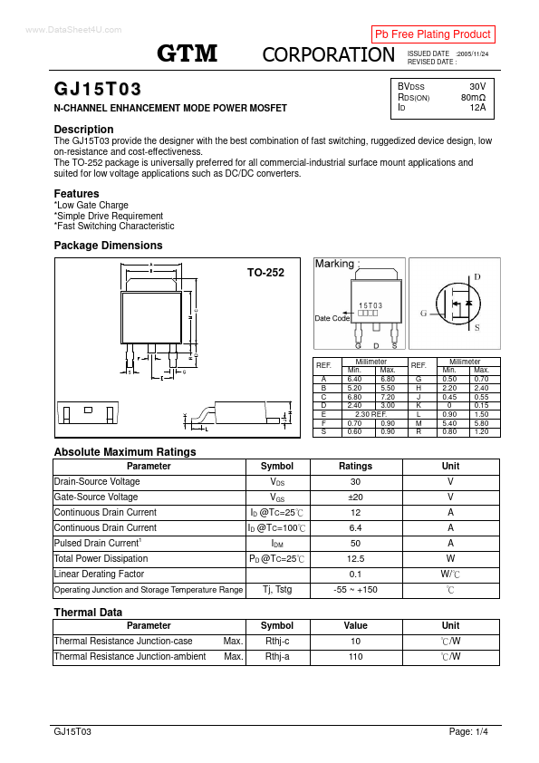
Package Dimensions
TO-252
REF.
A B C D E F S
Millimeter
Min.
Max....