GJ5103
GJ5103 is NPN HIGH SPEED SWITCHING TRANSISTOR manufactured by GTM.
Description
The GJ5103 is designed for high speed switching applications.
Features
- Low saturation voltage, typically VCE(sat) =0.15V at IC/IB=3A/0.15A
- High speed switching, typically tf =0.1 s at IC=3A
- Wide SOA
- plements to GJ1952
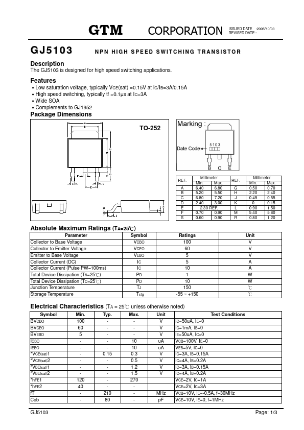
Package Dimensions
TO-252
Absolute Maximum Ratings (TA=25к)
Parameter
Symbol
Collector to Base Voltage
VCBO
Collector to Emitter Voltage
VCEO
Emitter to Base Voltage
VEBO
Collector Current (DC)
Collector Current (Pulse PW=100ms)
Total Device Dissipation (TA=25к)
Total Device Dissipation (TC=25к)
Junction Temperature
Storage Temperature
Tstg
REF.
A B C D E F S
Millimeter
Min.
Max....