GTM GSS6900S
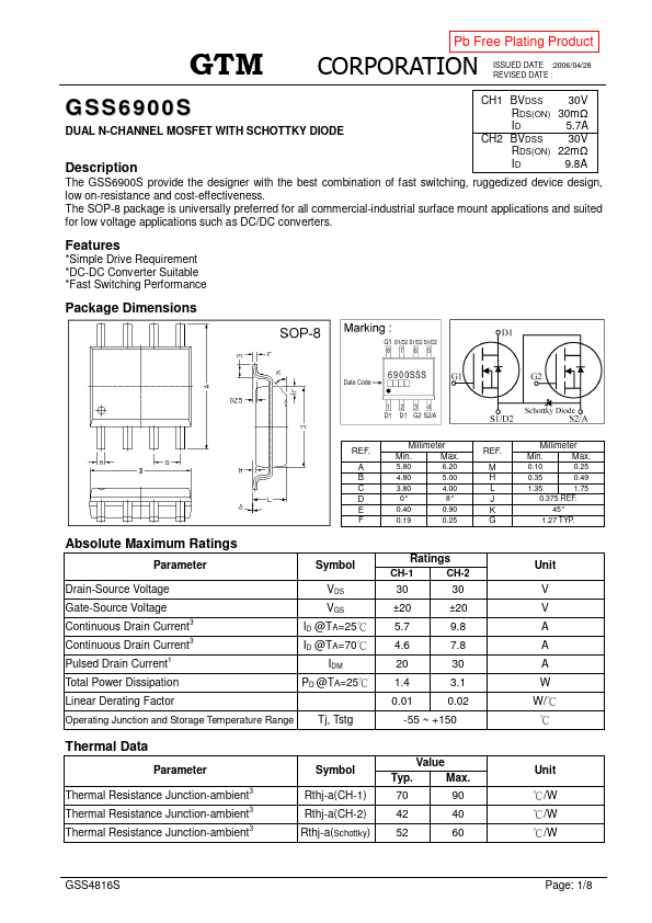
The GSS6900S provide the designer with the best combination of fast switching, ruggedized device design, low on-resistance and cost-effectiveness. The SOP-8 package is universally preferred for all commercial-industrial surface mount applications and suited for low voltage applications such as DC/DC converters.| Part No. | GSS6900S |
|---|---|
| Datasheet | GSS6900S Download |
| Manufacturer |  GTM |
| Description | Dual N-Channel MOSFET |
| Buy | Stock & Price |
DESCRIPTION
N-CH ID 9.8AFEATURES
*Simple Drive Requirement *DC-DC Converter Suitable *Fast Switching Performance Package Dimensions REF. A B C D E FABSOLUTE MAXIMUM RATINGS
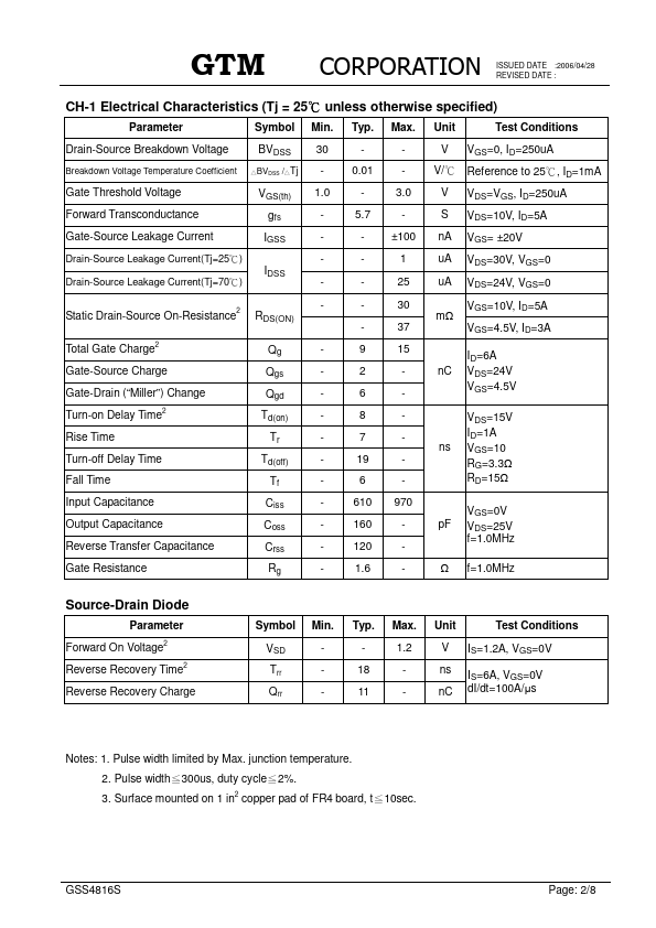
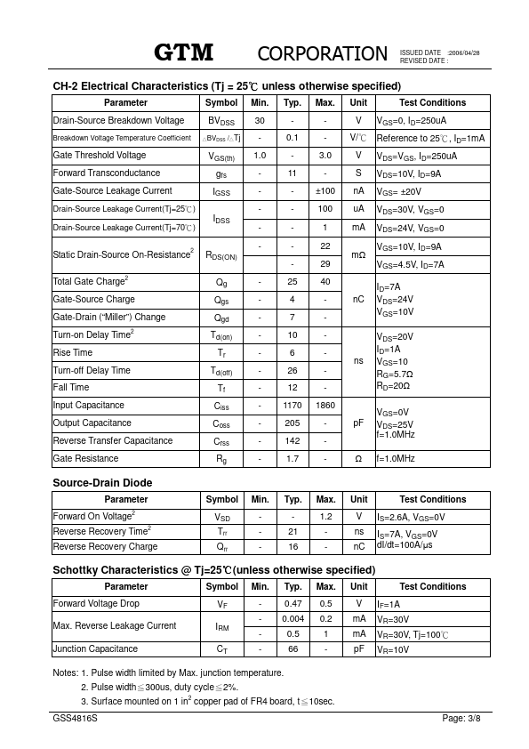
Parameter Symbol Drain-Source Voltage Gate-Source Voltage Continuous Drain Current3 Continuous Drain Current3 Pulsed Drain Current1 Total Power Dissipation VDS VGS ID @TA=25к ID @TA=70к IDM PD @TA=25к Linear Derating Factor Operating Junction and Storage Temperature Range Tj, Tstg Thermal Data Parameter Thermal Resistance Junction-ambient3 Thermal Resistance Junction-ambient3 Thermal Resistance Junction-ambient3 Symbol Rthj-a(CH-1) Rthj-a(CH-2) Rthj-a(Schottky) Millimeter Min. Max. 5.80 6.20 4.80 5.00 3.80 4.00 0° 8° 0.40 0.90 0.19 0.25 REF. M H L J K G Ratings CH-1 CH-2 30 30 ±20 ±20 5.7 9.8 4.6 7.8 20 30 1.4 3.1 0.01 0.02 -55 ~ +150 Value Typ. Max. 70 90 42 40 52 60 Millimeter Min. Max. 0.10 0.25 0.35 0.49 1.35 1.75 0.375 REF. 45° 1.27 TYP. Unit V V A A A W W/к к Unit к/W к/W к/W GSS4816S Page: 1/8 ISSUED DATE :2006/04/28 REVISED DATE : CH-1ELECTRICAL CHARACTERISTICS
(Tj = 25к unless otherwise specified) Parameter Symbol Min.