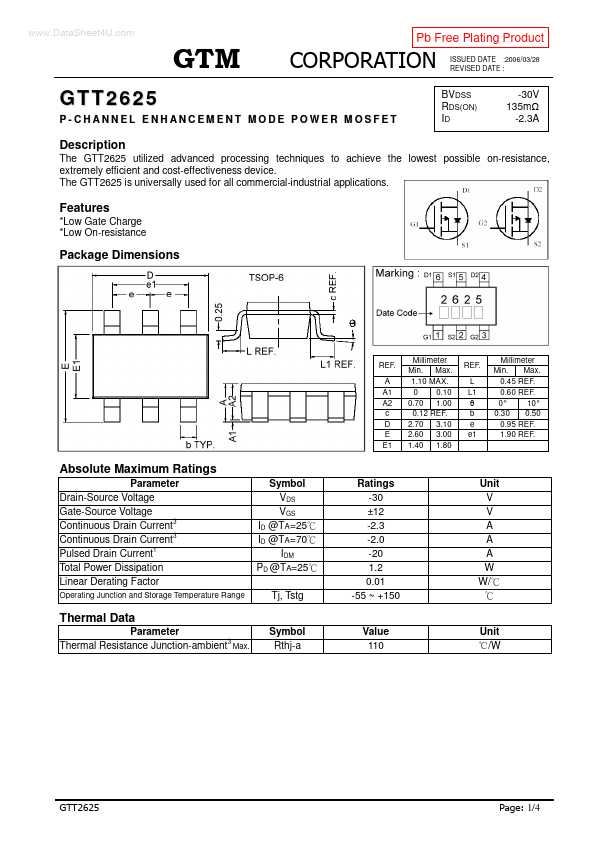
Datasheet4U Logo Datasheet4U.com

GTT2625 - P-CHANNEL ENHANCEMENT MODE POWER MOSFET

Description

Low Gate Charge Low On-resistance

Features

  • Package Dimensions REF. A A1 A2 c D E E1 Millimeter Min. Max. 1.10 MAX. 0 0.10 0.70 1.00 0.12 REF. 2.70 3.10 2.60 3.00 1.40 1.80 REF. L L1 b e e1 Millimeter Min. Max. 0.45 REF. 0.60 REF. 0° 10° 0.30 0.50 0.95 REF. 1.90 REF. Absolute Maximum Ratings Parameter Drain-Source Voltage Gate-Source Voltage Continuous Drain Current3 3 Continuous Drain Current Pulsed Drain Current1 Total Power Dissipation Linear Derating Factor Symbol VDS VGS ID @TA=25 ID @TA=70 IDM PD @TA=25 Tj, Tstg Symbol Rthj-a.

📥 Download Datasheet

Datasheet preview – GTT2625

Datasheet Details

Part number GTT2625
Manufacturer GTM
File Size 322.20 KB
Description P-CHANNEL ENHANCEMENT MODE POWER MOSFET
Datasheet download datasheet GTT2625 Datasheet
Additional preview pages of the GTT2625 datasheet.
Other Datasheets by GTM

Full PDF Text Transcription

Click to expand full text
www.DataSheet4U.com Pb Free Plating Product ISSUED DATE :2006/03/28 REVISED DATE : GTT2625 P-CHANNEL ENHANCEMENT MODE POWER MOSFET BVDSS RDS(ON) ID -30V 135m -2.3A The GTT2625 utilized advanced processing techniques to achieve the lowest possible on-resistance, extremely efficient and cost-effectiveness device. The GTT2625 is universally used for all commercial-industrial applications. Description *Low Gate Charge *Low On-resistance Features Package Dimensions REF. A A1 A2 c D E E1 Millimeter Min. Max. 1.10 MAX. 0 0.10 0.70 1.00 0.12 REF. 2.70 3.10 2.60 3.00 1.40 1.80 REF. L L1 b e e1 Millimeter Min. Max. 0.45 REF. 0.60 REF. 0° 10° 0.30 0.50 0.95 REF. 1.90 REF.
Published: |