GTT3585 Description
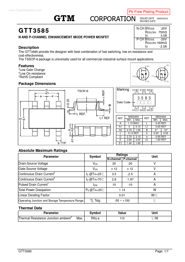
N-CH BVDSS 20V N-CH RDS(ON) 75m N-CH ID 3.5A P-CH BVDSS -20V N-CH RDS(ON) 160m N-CH ID -2.5A The GTT3585 provide the designer with best bination of fast switching, low on-resistance and cost-effectiveness. The TSSOP-6 package is universally used for all mercial-industrial surface mount applications.
GTT3585 Key Features
- Low Gate Change -Low On-resistance -RoHS pliant