General Semiconductor BS209
DMOS Transistors (P-Channel)
| Part No. | BS209 |
|---|---|
| Datasheet | BS209 Download |
| Manufacturer |  General Semiconductor |
| Description | DMOS Transistors (P-Channel) |
| Buy | Stock & Price |
FEATURES
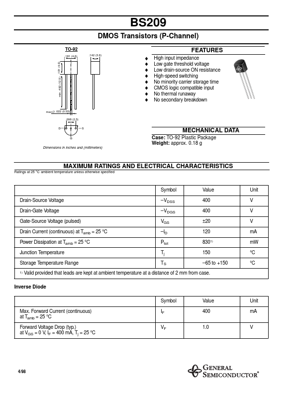
♦ ♦ ♦ ♦ ♦ ♦ ♦ ♦ High input impedance Low gate threshold voltage Low drain-source ON resistance High-speed switching No minority carrier storage time CMOS logic compatible input No thermal runaway No secondary breakdown max. ∅ .022 (0.55) .098 (2.5) D G SMECHANICAL DATA
Case: TO-92 Plastic Package Weight: approx. 0.18 g Dimensions in inches and (millimeters)MAXIMUM RATINGS AND ELECTRICAL CHARACTERISTICS
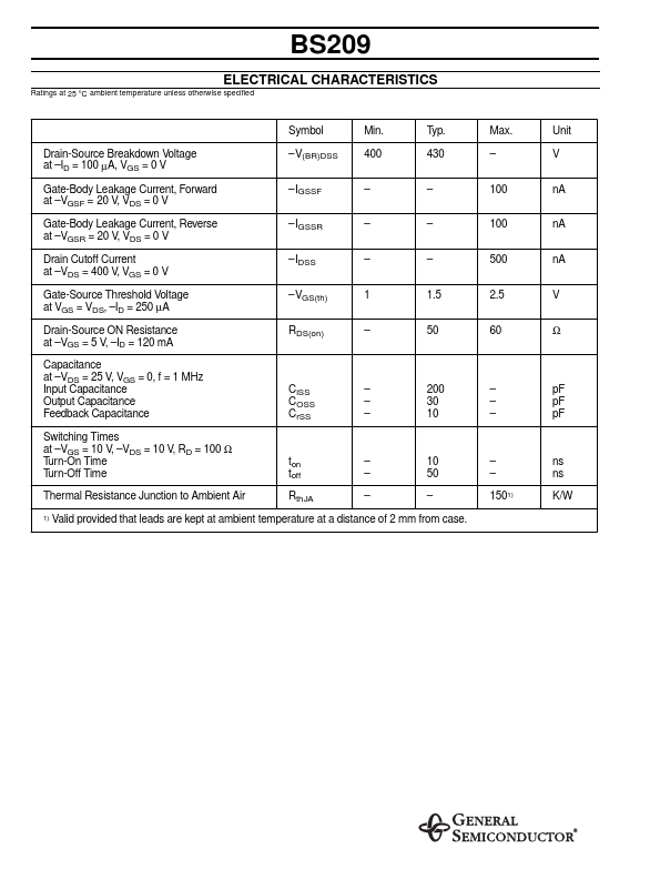
Ratings at 25 °C ambient temperature unless otherwise specified Symbol Drain-Source Voltage Drain-Gate Voltage Gate-Source Voltage (pulsed) Drain Current (continuous) at Tamb = 25 °C Power Dissipation at Tamb = 25 °C Junction Temperature Storage Temperature Range 1) Value 400 400 ±20 120 8301) 150 –65 to +150 Unit V V V mA mW °C °C –VDSS –VDGS VGS –ID Ptot Tj TS Valid provided that leads are kept at ambient temperature at a distance of 2 mm from case. Inverse Diode Symbol Max. Forward Current (continuous) at Tamb = 25 °C Forward Voltage Drop (typ.) at VGS = 0 V, IF = 400 mA, T...