GD16588
Description
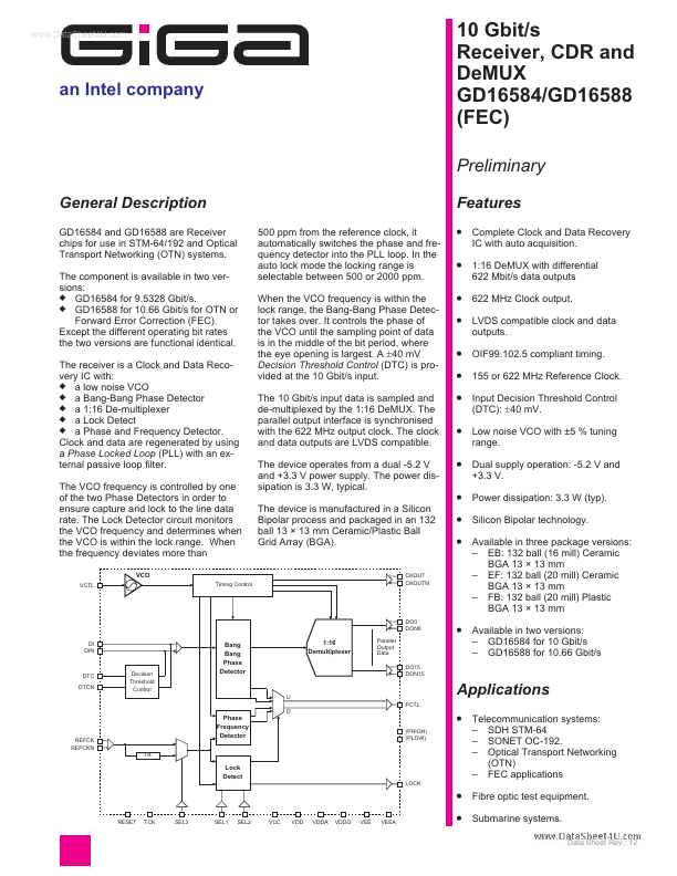
GD16584 and GD16588 are Receiver chips for use in STM-64/192 and Optical Transport Networking (OTN) systems. The ponent is available in two versions: u GD16584 for 9.5328 Gbit/s.
Key Features
- 500 ppm from the reference clock, it automatically switches the phase and frequency detector into the PLL loop
- In the auto lock mode the locking range is selectable between 500 or 2000 ppm
- When the VCO frequency is within the lock range, the Bang-Bang Phase Detector takes over
- It controls the phase of the VCO until the sampling point of data is in the middle of the bit period, where the eye opening is largest
- A ±40 mV Decision Threshold Control (DTC) is provided at the 10 Gbit/s input
- The 10 Gbit/s input data is sampled and de-multiplexed by the 1:16 DeMUX
- The parallel output interface is synchronised with the 622 MHz output clock
- The clock and data outputs are LVDS compatible
- The device operates from a dual -5.2 V and +3.3 V power supply
- The power dissipation is 3.3 W, typical