Good-Ark Semiconductor SSPL2015
This advanced technology has been especially tailored to minimize on-state resistance, provide superior switching performance, and withstand high energy pulse in the avalanche and commutation mode. These devices are well suited for high efficiency switch mode power supplies.| Part No. | SSPL2015 |
|---|---|
| Datasheet | SSPL2015 Download |
| Manufacturer |  Good-Ark Semiconductor |
| Description | N-Channel MOSFET |
| Buy | Stock & Price |
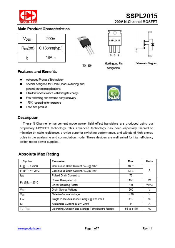
FEATURES AND BENEFITS
TO - 220● Advanced Process Technology
● Special designed for PWM, load switching and general purpose applications
● Ultra low on-resistance with low gate charge
● Fast switching and reverse body recovery
● 175℃ operating temperature
● Lead free product SSPL2015 200V N-Channel MOSFET Marking and Pin Assignment Schematic Diagram
DESCRIPTION
These N-Channel enhancement mode power field effect transistors are produced using our proprietary MOSFET technology. Absolute Max Rating Symbol ID @ TC = 25°C ID @ TC = 100°C IDM PD @TC = 25°C VDS VGS EAS IAS TJ TSTG Parameter Continuous Drain Current, VGS @ 10V Continuous Drain Current, VGS @ 10V Pulsed Drain Current ② Power Dissipation ③ Linear Derating Factor Drain-Source Voltage Gate-to-Source Voltage Single Pulse Avalanche Energy @ L=4.2mH Avalanche Current @ L=4.2mH Operating Junction and Storage Temperature Range Max. 18 ① 13 ① 72 150 1.0 200 ± 30 412 14 -55 to +175 Units A W W/°C V V mJ A °C Page 1 of 7 Rev.1.1 SSPL2015...