HM18DP02Q - P-Channel Enhancement Mode Field Effect Transistor
H&M Semiconductor
General Description
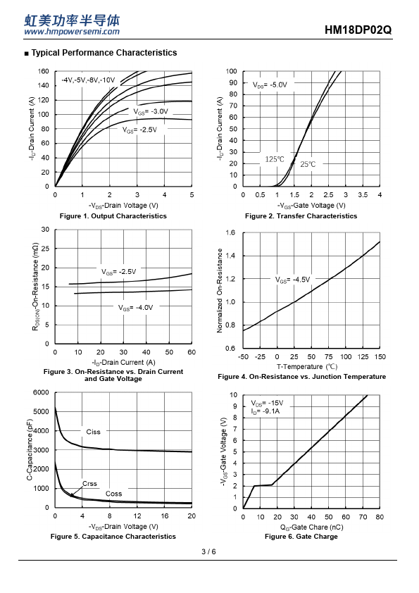
Trench Power MV MOSFET technology
High density cell design for Low RDS(ON)
High Speed switching
Applications
Battery protection
Load switch
Power management
Absolute Maximum Ratings (TA=25℃unless otherwise noted)
Parameter
Symbol
Maximum
Unit
Drain-so
The following content is an automatically extracted verbatim text
from the original manufacturer datasheet and is provided for reference purposes only.
View original datasheet text
HM18DP02Q
P-Channel Enhancement Mode Field Effect Transistor
DFN3.3X3.3
Product Summary
● VDS ● ID ● RDS(ON)( at VGS= -4.5V)
● RDS(ON)( at VGS= -2.5V)
-20V -18A <32mohm
<40mohm
General Description
● Trench Power MV MOSFET technology ● High density cell design for Low RDS(ON) ● High Speed switching
Applications
● Battery protection ● Load switch ● Power management
■ Absolute Maximum Ratings (TA=25℃unless otherwise noted)
Parameter
Symbol
Maximum
Unit
Drain-source Voltage
VDS
-20
V
Gate-source Voltage
VGS
Drain Current B
TA=25℃ @ Steady State TA=100℃ @ Steady State
ID
Drain Current B
TA=25℃ @ Steady State TA=70℃ @ Steady State
ID
Pulsed Drain Current A
IDM
±10
V
-18
A
-12.6
-18 -16.
 HM18DP02Q Datasheet