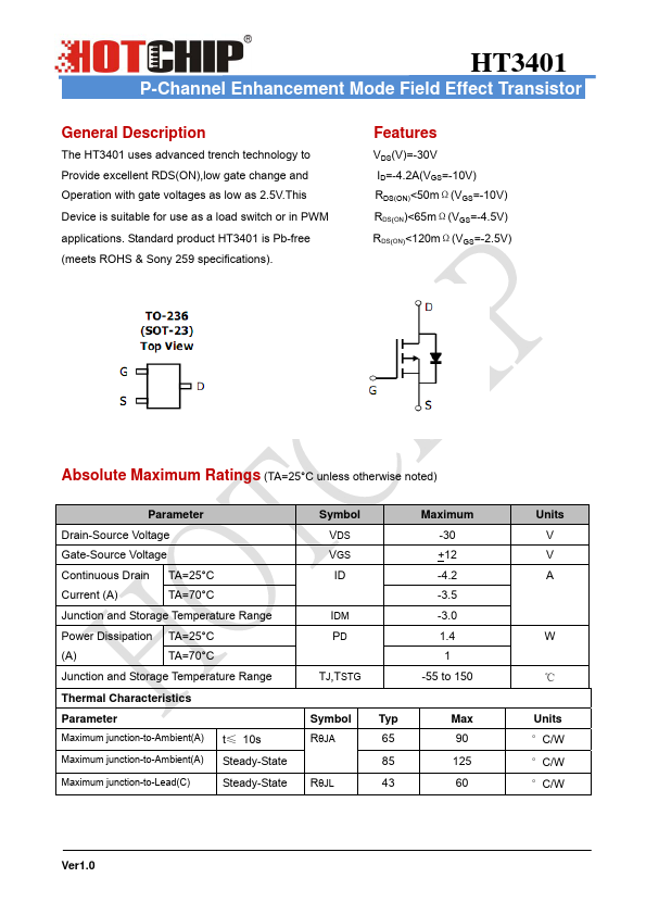
GENERAL DESCRIPTION
FEATURES
VDS(V)=-30V ID=-4.2A(VGS=-10V) RDS(ON)<50mΩ(VGS=-10V) RDS(ON)<65mΩ(VGS=-4.5V) RDS(ON)<120mΩ(VGS=-2.5V) ABSOLUTE MAXIMUM RATINGS
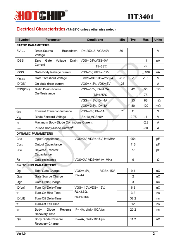
(TA=25°C unless otherwise noted) Parameter Drain-Source Voltage Gate-Source Voltage Continuous Drain TA=25°C Current (A) TA=70°C Junction and Storage Temperature Range Power Dissipation TA=25°C (A) TA=70°C Junction and Storage Temperature Range Thermal Characteristics Parameter Maximum junction-to-Ambient(A) Maximum junction-to-Ambient(A) Maximum junction-to-Lead(C) t≤ 10s Steady-State Steady-State Symbol VDS VGS ID IDM PD TJ,TSTG Symbol RθJA RθJL Typ 65 85 43 Maximum -30 +12 -4.2 -3.5 -3.0 1.4 1 -55 to 150 Max 90 125 60 Units V V A W ℃ Units °C/W °C/W °C/W Ver1.0 HT3401 ELECTRICAL CHARACTERISTICS
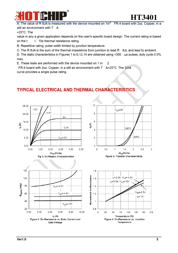
(TJ=25°C unless otherwise noted) Symbol Parameter Conditions Min STATIC PARAMETERS BVDSS Drain-Source Voltage Breakdown ID=-250µA, VGS=0V IDSS Zero Gate Voltage Drain VDS=-24V,VGS=0V Current TJ=55℃ -30 IGSS Gate-Body leakage current VDS=0... HOTCHIP