Datasheet Details
| Part number | HT3402 |
|---|---|
| Manufacturer | HOTCHIP |
| File Size | 271.62 KB |
| Description | 30V N-Channel MOSFET |
| Datasheet | HT3402-HOTCHIP.pdf |
|
|
|
Overview: OB2269 HT3402 30V N-Channel MOSFET General.
| Part number | HT3402 |
|---|---|
| Manufacturer | HOTCHIP |
| File Size | 271.62 KB |
| Description | 30V N-Channel MOSFET |
| Datasheet | HT3402-HOTCHIP.pdf |
|
|
|
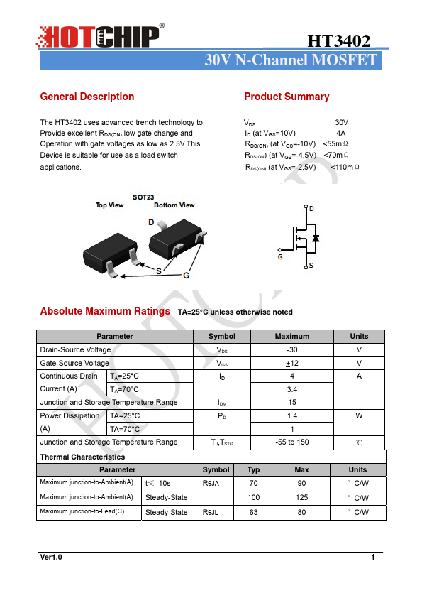
The HT3402 uses advanced trench technology to Provide excellent RDS(ON),low gate change and Operation with gate voltages as low as 2.5V.This Device is suitable for use as a load switch applications.
Product Summary VDS ID (at VGS=10V) RDS(ON) (at VGS=-10V) RDS(ON) (at VGS=-4.5V) RDS(ON) (at VGS=-2.5V) 30V 4A <55mΩ <70mΩ <110mΩ Absolute Maximum Ratings TA=25°C unless otherwise noted Parameter Drain-Source Voltage Gate-Source Voltage Continuous Drain TA=25°C Current (A) TA=70°C Junction and Storage Temperature Range Power Dissipation TA=25°C (A) TA=70°C Junction and Storage Temperature Range Thermal Characteristics Parameter Maximum junction-to-Ambient(A) Maximum junction-to-Ambient(A) Maximum junction-to-Lead(C) t≤ 10s Steady-State Steady-State Symbol VDS VGS ID IDM PD TJ,TSTG Symbol RθJA RθJL Typ 70 100 63 Maximum -30 +12 4 3.4 15 1.4 1 -55 to 150 Max 90 125 80 Units V V A W ℃ Units °C/W °C/W °C/W Ver1.0 1 HT3402 Electrical Characteristics (TJ=25°C unless otherwise noted) Symbol Parameter Conditions STATIC PARAMETERS BVDSS Drain-Source Breakdown Voltage ID=-250µA, VGS=0V IDSS Zero Gate Voltage Drain VDS=24V,VGS=0V Current TJ=55℃ IGSS VGS(th) ID(ON) RDS(ON) gFS VSD Is Gate-Body leakage current VDS=0V, VGS=±12V Gate Threshold Voltage VDS=VGS ID=-250µA On state drain current VGS=4.5V, VDS=5V Static Drain-Source On-Resistance VGS=10V, ID=4A TJ=125°C VGS=4.5V, ID=3A VGS=2.5V, ID=2A Forward Transconductance VDS=5V, ID=4A Diode Forward Voltage IS=1A,VGS=0V Maximum Body-Diode Continuous Current DYNAMIC PARAMETERS Ciss Input Capacitance Coss Output Capacitance Crss Reverse Transfer Capacitance Rg Gate resistance VGS=0V, VDS=-15V, f=1MHz VGS=0V, VDS=0V, f=1MHz SWITCHING PARAMETERS Qg Total Gate Charge VGS=4.5V, VDS=15V, ID=4A Qgs Gate Source Charge Qgd Gate Drain Charge tD(on) tr Turn-On DelayTime Turn-On Rise Time VGS=10V,VDS=15V, RL=3.75Ω, RGEN=6Ω tD(
| Part Number | Description |
|---|---|
| HT3402S | 40V/2A Constant Voltage & Constant Current Buck Converter |
| HT3401 | P-Channel Enhancement Mode Field Effect Transistor |
| HT3406 | 1.5MHz Synchronous Buck Regulator |
| HT3420 | 2A 28V Synchronous Buck Converter |
| HT3540S | Single-cell Li-ion battery charger |
| HT3550 | Single-cell lithium battery charge management |
| HT3560 | Single-cell lithium-ion battery charge management |
| HT358 | QUADRUPLE OPERATIONAL AMPLIFIERS |
| HT3582D | universal charger controller |
| HT3582DA | universal charger controller |