DESCRIPTION
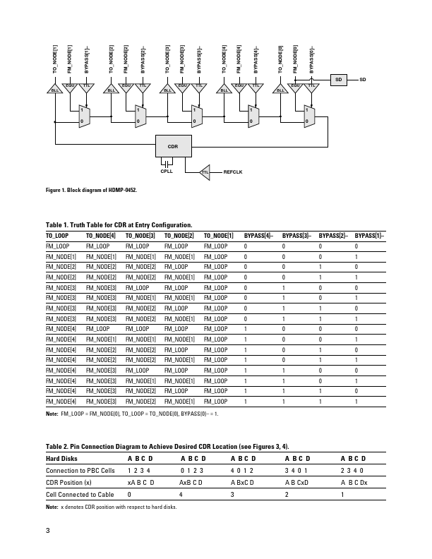
Port Bypass Circuits are used in hard disk arrays constructed in Fibre Channel Arbitrated Loop (FC-AL) configurations. A Port Bypass Circuit (PBC) consists of multiple 2:1 multiplexers daisy chained along with a CDR. Each port has two modes of operation: “disk in loop” and “disk bypassed”. When the “disk in loop” mode is selected, the loop goes into and out of the disk drive at that port. For example, data goes from the HDMP-0452’s TO_NODE[n]± differential output pins to the Disk Drive Transceiver IC’s (e.g., an HDMP-1536A) Rx± differential input pins. Data from the Disk Drive Transceiver IC’s Tx± differential outputs goes to the HDMP-0452’s FM_NODE[n]± differential input pins. Figures 3 and 4 show connection diagrams for disk drive array applications. When the “disk bypassed” mode is selected, the disk drive is either absent or nonfunctional and the loop bypasses the hard disk. The “disk bypassed” mode is enabled by pulling the BYPASS[n]– pin low. Leave BYPASS[n]– floating to enable the “disk in loop” mode. Hewlett-Packard