RFD16N03LSM Overview
Key Specifications
Max Operating Temp: 175 °C
Description
The RFD16N03L and RFD16N03LSM are N-channel power MOSFETs manufactured using the MegaFET process. This process, which uses feature sizes approaching those of LSI circuits, gives optimum utilization of silicon, resulting in outstanding performance.
Key Features
- rDS(ON) = 0.022Ω
- Temperature Compensating PSPICE Model
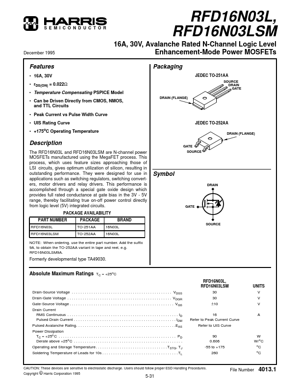
- Can be Driven Directly from CMOS, NMOS, and TTL Circuits DRAIN (FLANGE) JEDEC TO-251AA SOURCE DRAIN GATE
- Peak Current vs Pulse Width Curve
- UIS Rating Curve
- +175oC Operating Temperature JEDEC TO-252AA DRAIN (FLANGE)