Datasheet4U Logo Datasheet4U.com

HWC34NC Datasheet C-Band Power FET Non-Via Hole Chip

Manufacturer: Hexawave

Datasheet Details

Part number HWC34NC
Manufacturer Hexawave
File Size 74.28 KB
Description C-Band Power FET Non-Via Hole Chip
Datasheet download datasheet HWC34NC Datasheet

General Description

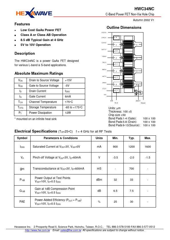
The HWC34NC is a power GaAs FET designed for various L-band & S-band applications.

Absolute Maximum Ratings VDS VGS ID IG TCH TSTG PT* Drain to Source Voltage Gate to Source Voltage Drain Current Gate Current Channel Temperature Storage Temperature Power Dissipation * mounted on an infinite heat sink +15V -5V IDSS 6mA 175°C -65 to +175°C 12W Autumn 2002 V1 Outline Dimensions 1525.0 1392.5 9 1235.0 1077.5 1 10 5 920.0 762.5 2 11 6 605.0 3 7 447.5 12 290.0 132.5 0.0 4 13 8 0.0 75.5 444.5 524.0 Units: µm Thickness: 100 ±5 Chip size ±50 Bond Pads 1-4 (Gate): Bond Pads 5-8 (Drain): Bond Pads 9-13(Source): 100 x 100 100 x 100 100 x 100 Electrical Specifications (TA=25°C) f = 4 GHz for all RF Tests Symbol Parameters & Conditions Units Min.

Typ.

Overview

HWC34NC C-Band Power FET Non-Via Hole Chip.

Key Features

  • Low Cost GaAs Power FET.
  • Class A or Class AB Operation.
  • 8.5 dB Typical Gain at 4 GHz.
  • 5V to 10V Operation.