The following content is an automatically extracted verbatim text
from the original manufacturer datasheet and is provided for reference purposes only.
View original datasheet text
2SJ363
Silicon P-Channel MOS FET
Application
Low frequency power switching
Features
• Low on-resistance • Low drive current • 4 V gate drive device can be driven from 5 V source
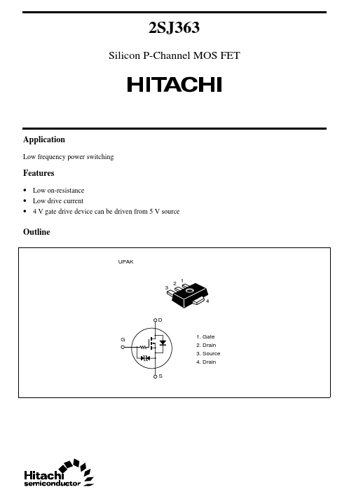
Outline
UPAK 2 1 4 D 1. Gate 2. Drain 3. Source 4. Drain S
3
G
2SJ363
Absolute Maximum Ratings (Ta = 25°C)
Item Drain to source voltage Gate to source voltage Drain current Drain peak current Body to drain diode reverse drain current Channel dissipation Channel temperature Storage temperature Symbol VDSS VGSS ID I D(pulse)* I DR Pch* Tch Tstg
2 1
Ratings –30 ±20 –2 –4 –2 1 150 –55 to +150
Unit V V A A A W °C °C
Notes: 1. PW ≤ 100 µs, duty cycle ≤ 10% 2. Value on the alumina ceramic board (12.5×20×0.7 mm) 3. Marking is “PY”.